

Light processing method for preparing conducting micro-nano structure by utilizing graphene oxide
A technology of micro-nano structure and micro-nano processing, applied in the direction of micro-structure technology, micro-structure device, nano-structure manufacturing, etc., can solve the problems that cannot meet the high precision, three-dimensional and complex patterning of graphene micro-nano structure, and achieve convenient Achieved effect
- Summary
- Abstract
- Description
- Claims
- Application Information
AI Technical Summary
Problems solved by technology
Method used
Image

Examples
Embodiment 1
[0038] (1) Synthesize graphene oxide material and prepare graphene oxide film.
[0039] Graphene oxide materials were prepared by the Hummers method. In a 1000ml three-necked flask, add 10g of graphite powder (with a size less than 150um) and 230ml of concentrated sulfuric acid with a mass concentration of 98% under the condition of an ice-water bath at 0°C. Then add 30 g of potassium permanganate into the three-necked flask in 10 times within 1 hour, and control the reaction temperature within 20°C. After the addition was complete, the stirring reaction was continued for 1 hour. Then slowly add 700ml of deionized water into the three-neck flask, control the temperature at about 38°C, and stir for 2 hours. Afterwards, the mixture was transferred into a 2000ml beaker, and after diluting the reaction solution with 1.5L deionized water, 25ml of H 2 o 2 At this time, the reaction solution changed from yellowish brown to golden yellow. Filtrate while hot, fully wash with 5% HC...
Embodiment 2
[0050] 1) Synthesize graphene oxide material and prepare graphene oxide film.
[0051] The steps of synthesizing graphene oxide and preparing graphene solution are the same as in Example 1. But make the electrodes first and then prepare the graphene film on the electrodes. The substrate was a gold film with a channel on the surface of the cover glass (the channel width was 100 μm). The substrate was prepared by combining mask and vacuum thermal deposition methods. The template used is a wire template. A gold wire with a diameter of 100um is wound on a cover glass with a thickness of 170um for masking. The winding method is as follows: Figure 5 As shown in (a), a gold film is evaporated on the surface of the cover glass by vacuum thermal deposition. The equipment used is a vacuum coating machine produced by Shenyang Sida Company. In the vacuum chamber, gold wire is used as the gold source, and the gold wire is vaporized into gas by heating. Gold, deposited on a coverslip wi...
Embodiment 3
[0066] 1) Synthesize graphene oxide material, prepare graphene oxide thin film; This step is identical with embodiment 1.
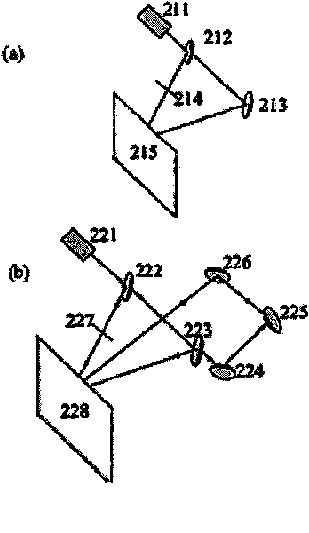
[0067] 2) Build a dual-beam interference laser processing system.
[0068] The schematic diagram of the optical path of the two-beam interference system is as follows figure 2 (a) shown. The wavelength of the laser light source is 355nm, the pulse width is 10ns, and the repetition frequency is 10Hz. The laser beam passes through the beam splitter 212 (30% reflection, 70% transmission), and the transmitted light passes through the beam splitter 213. A neutral beam is added to the reflected light path. Variable density filter 214, when the density is 30%, the light intensity of the two beams of interference light is equal, used for interference processing.
[0069] 3) Laser double-beam interference to obtain graphene grating structure.
[0070] The angles of the beam splitter 212 and the beam splitter 213 are adjusted so that the graphene oxide film to ...
PUM
| Property | Measurement | Unit |
|---|---|---|
| Line width | aaaaa | aaaaa |
| Diameter | aaaaa | aaaaa |
| Thickness | aaaaa | aaaaa |
Abstract
Description
Claims
Application Information