Method for preparing copper barrier layer-seed crystal layer film

A kind of thin film preparation, barrier layer technology

Active Publication Date: 2010-06-30
BEIJING NAURA MICROELECTRONICS EQUIP CO LTD
View PDF0 Cites 7 Cited by
  • Summary
  • Abstract
  • Description
  • Claims
  • Application Information

AI Technical Summary

Problems solved by technology

[0014] The barrier layer deposition chamber technology is complex and expensive. At the same time, the increase in particles caused by the addition of tantalum heavy sputtering coils reduces the production yield of the system; the equipment for realizing the reactive pre-cleaning technology has a complex structure and high prices; reaction, the possibility of contamination of the substrate is relatively high

Method used


Image

  • Method for preparing copper barrier layer-seed crystal layer film
  • Method for preparing copper barrier layer-seed crystal layer film
  • Method for preparing copper barrier layer-seed crystal layer film

Examples


specific Embodiment 1

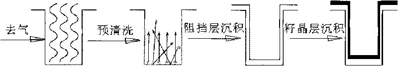
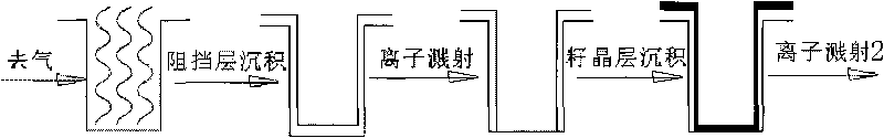
[0032] The production process of the copper barrier layer / seed layer film is: degassing => barrier layer deposition => ion sputtering => seed layer deposition => secondary ion sputtering 2.

[0033] First, carry out the degassing process;

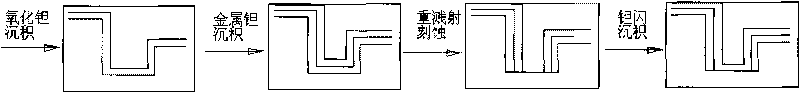
[0034] Next, a barrier layer deposition process is performed: first depositing a tantalum nitride film, and then depositing a metal tantalum film. After the tantalum nitride / tantalum double-layer barrier film deposition process is performed, there are impurity layers such as copper oxide and a tantalum nitride / tantalum double-layer barrier layer on the surface of the lower copper metal at the bottom of the through hole in sequence;

[0035] Subsequently, the ion sputtering process step is carried out. By sputtering, the above two layers of substances will be removed at the same time, exposing the underlying metal surface; moreover, ion sputtering will play the role of heavy sputtering technology, which will have a positive effect on the met...

specific Embodiment 2

[0040] The production process of the copper barrier layer / seed layer film is: degassing => barrier layer deposition => ion sputtering => seed layer deposition. Wherein, the process conditions of the ion sputtering process steps are: the power of the upper radio frequency is 300-800W, the power of the lower radio frequency is 200-700W, and the flow rate of argon gas is 20-150 sccm.

[0041] Compared with the specific embodiment 1, the process steps are simplified, and the dual effects of pre-cleaning and optimizing the pore filling coverage of the barrier film can be satisfied.

[0042] The invention adopts simplified barrier layer chamber design and barrier layer deposition process, which reduces the cost; at the same time, it avoids the problem of particle increase caused by the addition of tantalum heavy sputtering coils;

[0043] Using low-cost ion sputtering pre-cleaning technology, through the optimization of the process flow, the equipment and chip manufacturing costs ar...


PUM


Abstract

The invention discloses a method for preparing a copper barrier layer-seed crystal layer film, which includes the steps of forming a through hole and a groove on a substrate at first, and performing deaeration treatment on the through hole and the groove; then depositing a tantalum nitride film and an antalum film; performing ion sputtering and finally depositing a seed crystal layer. The pre-cleaning step and re-sputtering step can be omitted through the ion sputtering step, which simplifies process and equipment and cannot generate pollution to the substrate. The method for preparing the copper barrier layer-seed crystal layer film can be applied to an interconnection process between copper and dual damascene with technical nodes below 45nm to expand the technical nodes below 32nm and avoid the expenses for updating ship manufacturing equipment when expanding to smaller technical nodes.

Description

technical field [0001] The invention relates to a semiconductor processing technology, in particular to a method for preparing a copper barrier layer-seed layer thin film. Background technique [0002] As the dimensions of CMOS transistors continue to shrink to the sub-micron level, the number of transistors in high-efficiency, high-density integrated circuits rises to tens of millions. The signal integration of these large number of active components requires high-density metal wiring, but the resistance and parasitic capacitance brought by these metal interconnections have become the main factors limiting the speed of this efficient integrated circuit. [0003] At present, the semiconductor industry uses metal copper interconnection wires, which reduces the resistance between metal wiring layers and enhances circuit stability; at the same time, low dielectric constant dielectric materials are used instead of silicon dioxide as the insulating medium between metal layers, re...

Claims


Application Information

Patent Timeline
Patent Type & Authority Applications(China)
IPC IPC(8): H01L21/768H01L21/3205C23C14/34
Inventor 杨柏
Owner BEIJING NAURA MICROELECTRONICS EQUIP CO LTD
Why Eureka
Try Eureka