Grooved field-effect tube and preparation method thereof

A field effect transistor and trench technology, applied in the field of field effect transistors and trench field effect transistors, can solve the problems of increasing gate-drain capacitance Cgd, reducing switching speed, increasing switching power consumption, etc., and improving roughness. , The effect of improving device performance and improving switching speed

Inactive Publication Date: 2010-06-30
GRACE SEMICON MFG CORP
View PDF0 Cites 17 Cited by
  • Summary
  • Abstract
  • Description
  • Claims
  • Application Information

AI Technical Summary

Problems solved by technology

[0004] Figure 1b It is a schematic diagram of the parasitic elements in the trench field effect transistor 100 unit structure, Figure 1c It is the equivalent circuit diagram of trench field effect transistor 100 with parasitic elements, such as 1b and Figure 1c As shown, the input capacitance Ciss=Cgs+Cgd when the drain and the source are shorted, the output capacitance Coss=Cds+Cgd when the gate and the source are shorted, and the reverse transmission when the gate and the source are shorted Capacitance Crss=Cgd, with the increase of the reciprocal, the gate charge Qg per unit area increases, and the gate-to-drain capacitance Cgd increases, thereby increasing the switching power consumption and reducing the switching speed

Method used


Image

  • Grooved field-effect tube and preparation method thereof
  • Grooved field-effect tube and preparation method thereof
  • Grooved field-effect tube and preparation method thereof

Examples


Embodiment Construction

[0029] In order to make the objectives, technical solutions and advantages of the present invention clearer, the present invention will be further described in detail below with reference to the accompanying drawings.

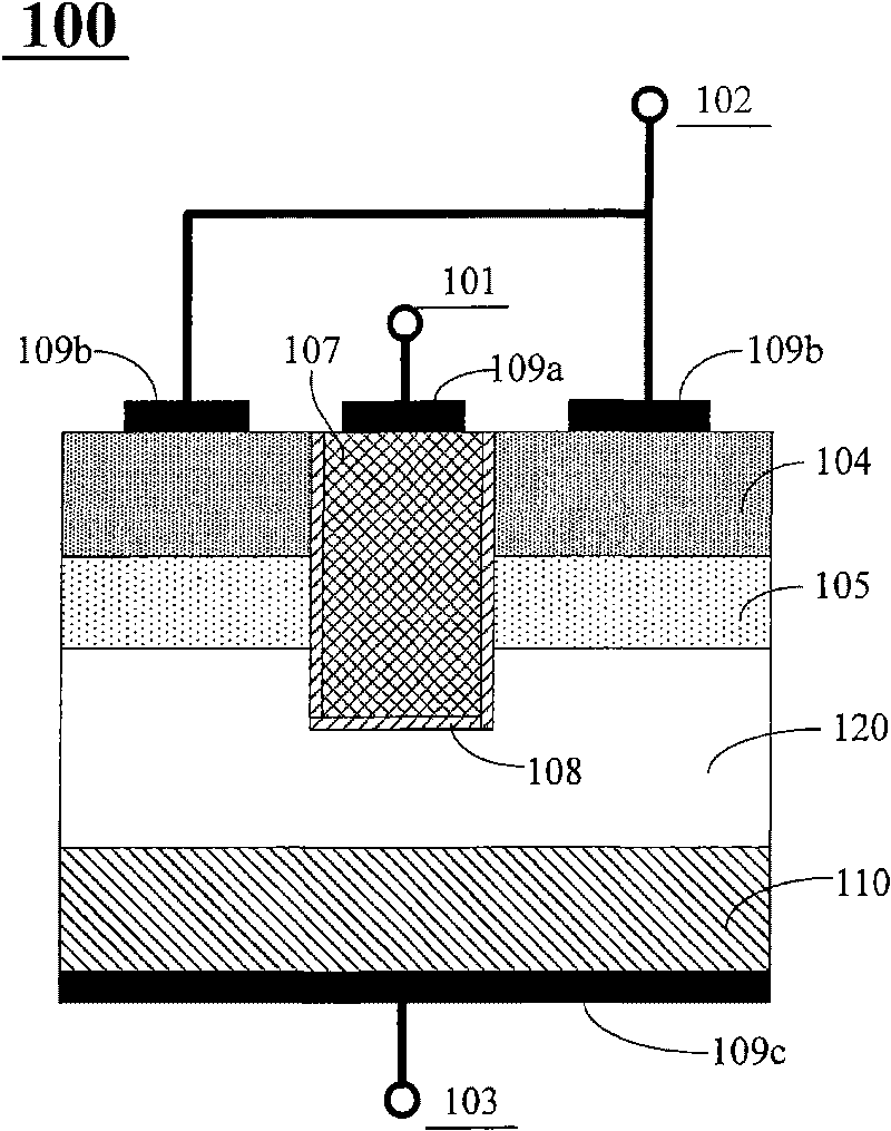
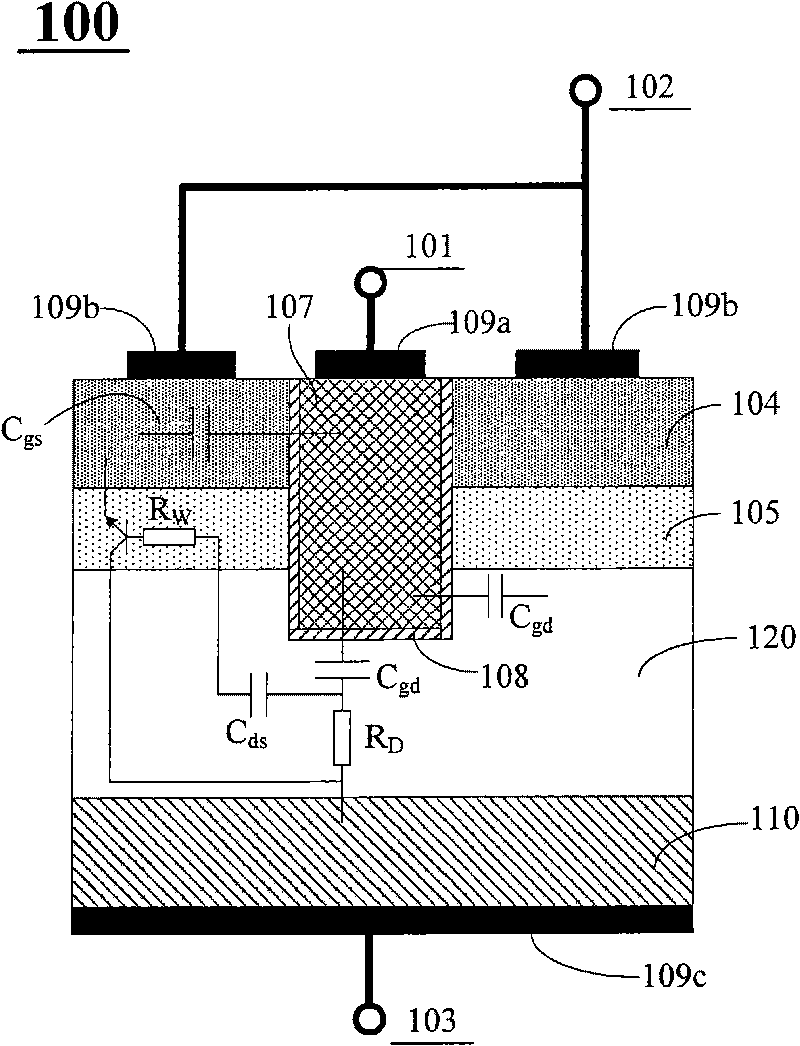
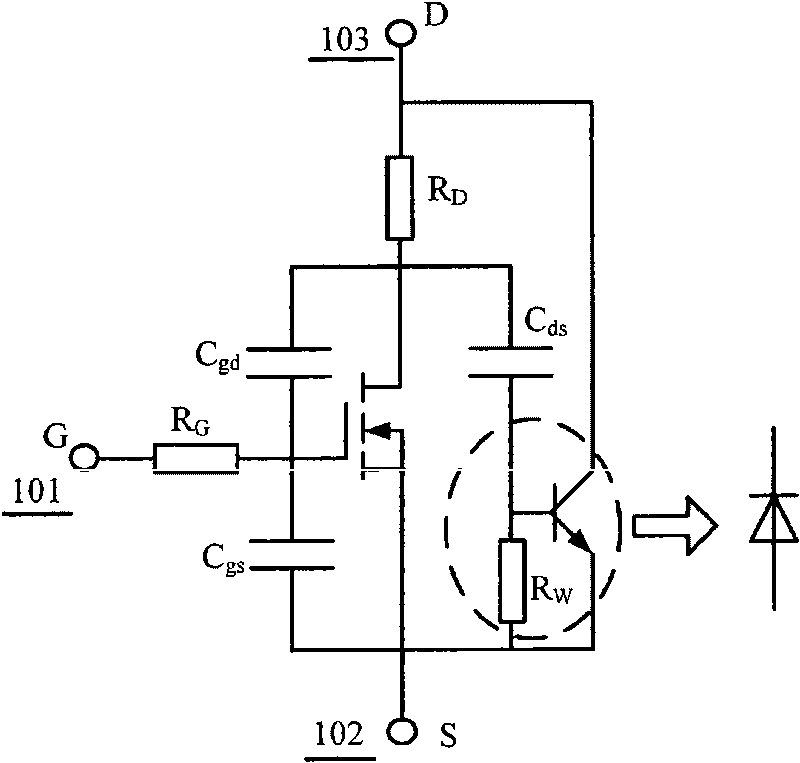
[0030] figure 2 It is a schematic cross-sectional structure diagram of the trenched field effect transistor provided by the present invention.

[0031] like figure 2 As shown, the trench FET 200 includes: a semiconductor substrate 210 of a first conductivity type and an epitaxial layer 220 of the first conductivity type covering its upper surface, and a source doping of the first conductivity type located in the epitaxial layer 210 Region 201 and channel region 202 of the second conductivity type, trench polysilicon gate 204 surrounded by source doping region 201 and channel region 202, respectively used to separate trench polysilicon gate 204 from the active region and the body region side spacers 207 and gate oxide layer 205, source / drain / gate electrodes ...


PUM


Abstract

The invention relates to a grooved field-effect tube and a preparation method thereof, belonging to the field of semiconductor devices; an insulation layer with thicker thickness is led in between a gate oxide at bottom part of the groove and a polysilicon gate of the groove, so as to increase the relative distance among the polysilicon gate, an extension layer and a substrate layer used as a drain region, that is, the distance between two electrode plates of a gate-drain capacitance is increased, therefore, the gate-drain capacitance of the grooved field-effect tube is reduced, the charging and discharging time of the field-effect tube to the gate-drain capacitance is greatly shortened in the switching process, the switching speed of the grooved field-effect tube is improved, dynamic loss is reduced and the performance of the devices are greatly improved on the premise of not changing the polysilicon gate area and not increasing the conduction resistance.

Description

technical field [0001] The invention relates to a field effect transistor, in particular to a vertical structure trench type field effect transistor, which belongs to the technical field of semiconductors. Background technique [0002] As a new type of high-power MOS field effect transistor developed on the basis of the planar MOS field effect transistor, the power trench MOS field effect transistor eliminates the parasitic JFET effect of the planar MOS field effect transistor and has a reduced on-resistance. , saturation voltage reduction, fast switching speed, high channel density, small chip size, etc., are the mainstream of the development of medium and low voltage high power MOS field effect transistors. [0003] Figure 1a It is a schematic cross-sectional structure diagram of a common trench FET 100 . like Figure 1a shown, the trench FET 100 is in N + A layer of N- epitaxial layer 120 is grown on the silicon substrate 110, and electrons are formed by N + The sourc...

Claims


Application Information

Patent Timeline
Patent Type & Authority Applications(China)
IPC IPC(8): H01L29/78H01L21/336
Inventor 刘宪周克里丝彭树根张雨
Owner GRACE SEMICON MFG CORP
Why Eureka
Try Eureka