

Compound semiconductor material doped with rare-earth elements and growth method thereof
A rare earth element and semiconductor technology, applied in the field of semiconductor materials, can solve the problems of reducing the luminous performance of GaN crystals and large lattice distortion, and achieve the effects of improving lattice distortion and improving luminous efficiency.
- Summary
- Abstract
- Description
- Claims
- Application Information
AI Technical Summary
Problems solved by technology
Method used
Image

Examples
no. 1 Embodiment approach
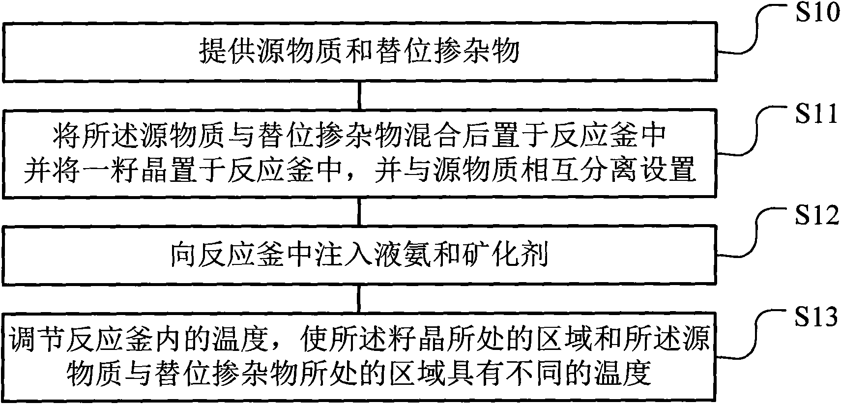
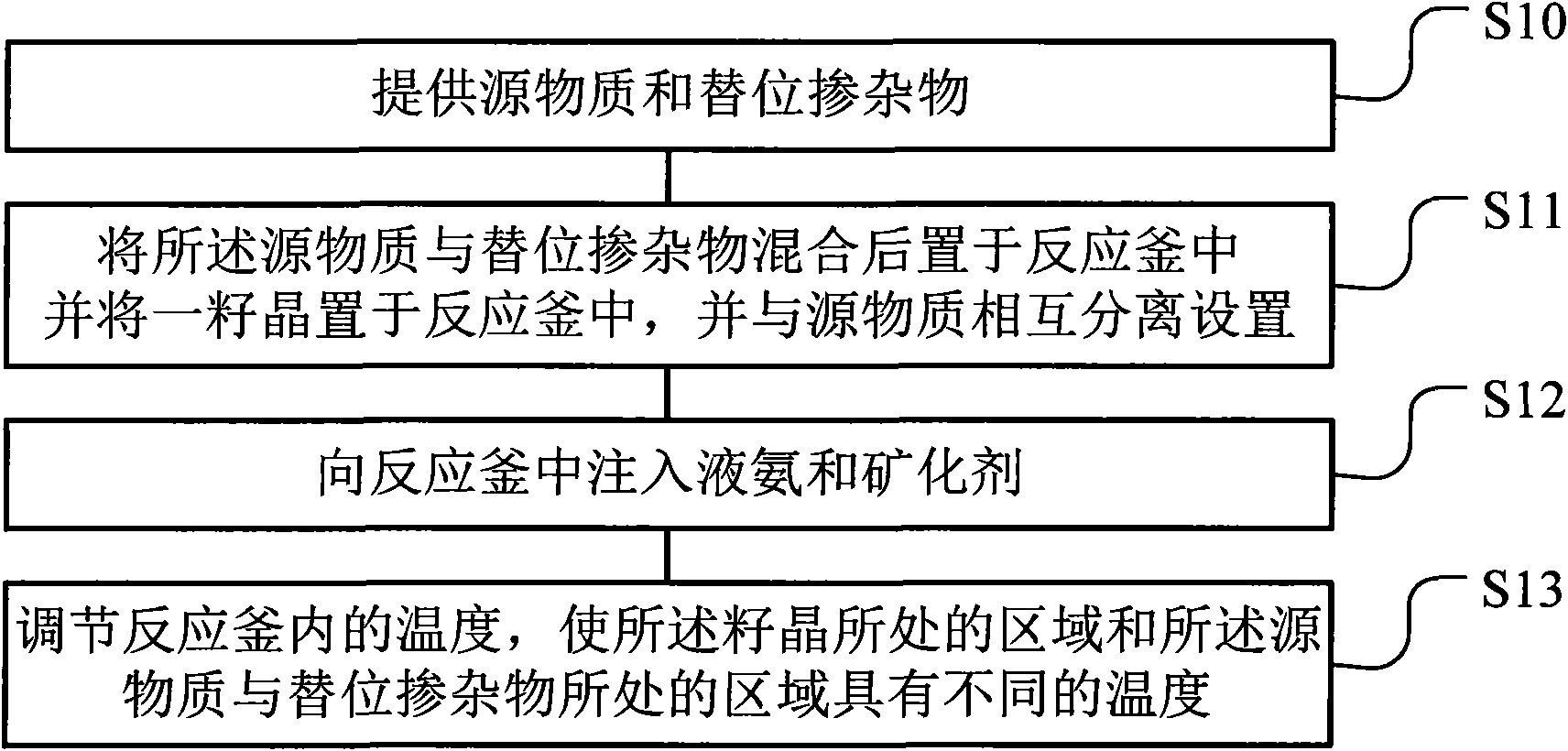
[0025] attached figure 1 Shown is a schematic diagram of the implementation steps of this specific embodiment, including: step S10, providing the source material and the replacement dopant; step S11, mixing the source material and the replacement dopant, placing them in the reaction vessel, and A seed crystal is placed in the reaction kettle, and is separated from the source material; step S12, injecting liquid ammonia and mineralizer into the reaction kettle; step S13, adjusting the temperature in the reaction kettle so that the seed crystal is in The region of and the region where the source material and the replacement dopant are located have different temperatures.
[0026] First, referring to step S10, a source material and a replacement dopant are provided, the source material is a mixture of one or more Group III elements and one or more rare earth elements, and the replacement dopant is a Group III elements or a mixture of multiple group III elements, and the atomic num...
no. 2 Embodiment approach
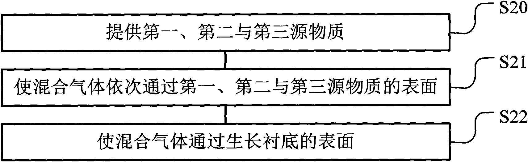
[0044] attached figure 2 Shown is a schematic diagram of the implementation steps of this specific embodiment, including: step S20, providing the first, second and third source substances; step S21, making the mixed gas pass through the surfaces of the first, second and third source substances in sequence; Step S22, passing the mixed gas over the surface of the growth substrate.
[0045] First, referring to step S20, first, second and third source materials are provided, wherein the second source material is selected from Ce, Pr, Nd, Pm, Sm, Eu, Gd, Tb, Dy, Ho, Er, Tm and Yb One or more of them, the first source material is selected from one or more of B, Al, Ga and In, the third source material is selected from one or more of B, Al, Ga and In species, and the atomic number of the elements contained in the third source material is less than the atomic number of the elements contained in the first source material;
[0046] The function of the third source substance is as a s...
Embodiment 1
[0058] In this example, x=0.1%, y=0.01%, Re is the rare earth metal Er, and A is the metal boron B. Put the above-mentioned weighed raw materials in the evaporation pool of the HVPE device, select the sapphire with GaN film as the substrate, control the temperature of the Ga evaporation pool at 850°C, control the Er evaporation pool at 850°C, The temperature is controlled at 900°C. to N 2 / H 2 The mixed gas as carrier gas, with NH 3As a nitrogen source, HCl as a reaction gas flows through three evaporation pools filled with Ga, rare earth metal Er, and metal boron respectively. get 50
[0059] um thick crystal film, cooling the substrate and each evaporation pool to room temperature, the rare earth ions and B can be taken out 3+ Co-doped GaN crystal film. B 3+ Doped with the same concentration of Er 3+ GaN crystal film, the fluorescence intensity is enhanced by 5%-20%.
PUM
 Abstract
Description
Claims
Application Information