Method for manufacturing light-emitting diode chip

A technology of light-emitting diodes and manufacturing methods, which is applied in the direction of electrical components, circuits, semiconductor devices, etc., can solve the problems of optoelectronic device performance such as forward voltage, light intensity, reverse leakage current wavelength uniformity, FWHM influence, etc., to achieve improvement Internal quantum efficiency, reduction of crystal defects, obvious effect

Active Publication Date: 2010-07-28
EPILIGHT TECH
View PDF4 Cites 24 Cited by
  • Summary
  • Abstract
  • Description
  • Claims
  • Application Information

AI Technical Summary

Problems solved by technology

However, the residual stress and crystal defects in the epitaxial growth chip structure still have a great influence on the performance of optoelectronic devices such as forward voltage, light intensity, reverse leakage current, wavelength uniformity, FWHM, etc.

Method used


Image

  • Method for manufacturing light-emitting diode chip
  • Method for manufacturing light-emitting diode chip
  • Method for manufacturing light-emitting diode chip

Examples


Embodiment 1

[0031] Please see Figure 1-4 , the manufacturing method of the light-emitting diode chip that embodiment one provides comprises the following steps:

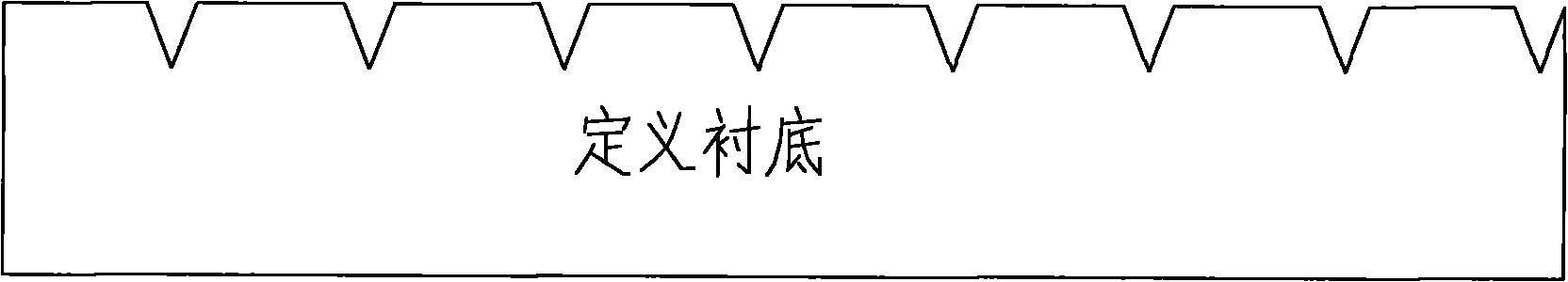
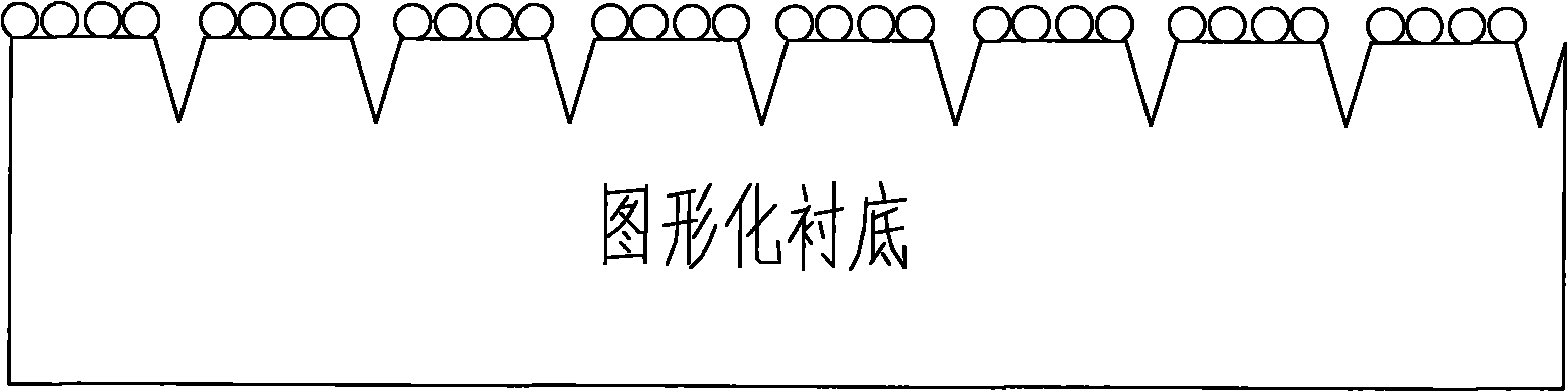
[0032] Step A, such as figure 1 , figure 2 As shown, first, aisles are formed on the surface of the growth substrate by photolithography and etching (such as plasma etching) or laser scribing, and the aisles directly divide the surface of the growth substrate into small areas with the same size as the final chip. Define the size of the chip (define the substrate), and the depth of the formed aisle is 15-50 microns; the preferred range of the general aisle depth is 15-20 microns, and the preferred aisle depth is about 20 microns. The growth substrate may be a Si substrate, a SiC substrate, a sapphire substrate, etc., and a sapphire substrate is preferred in this embodiment. The size of the growth substrate is more than 2 inches, and the beneficial effect of the present invention on large-size substrates will be more obvious....

Embodiment 2

[0041]See also Figure 1-4 , the manufacturing method of the light-emitting diode chip that embodiment 2 provides comprises the following steps:

[0042] Step A, first utilize processes such as laser scribing to form aisles on the surface of the growth substrate, and the aisles directly divide the surface of the growth substrate into small areas (defined as substrates) with the same size as the final chip, and the depth of the aisles formed is 15- 50 microns; generally, the preferred range of aisle depth is 15-20 microns, and the preferred aisle depth is about 20 microns. The growth substrate may be a SiC substrate, a sapphire substrate, etc., and a sapphire substrate is preferred in this embodiment. The size of the growth substrate is more than 2 inches, and a growth substrate of 2 inches is used in this embodiment.

[0043] Step B, cleaning the growth substrate after step A, and removing the remaining dirt in the aisle. The cleaning method can be laser cleaning, or using h...


PUM


Abstract

The invention discloses a method for manufacturing a light-emitting diode chip, which comprises the following steps: firstly forming a corridor on the surface of a growth substrate, dividing the surface of the growth substrate into a small region which is in the same size with the final chip, and defining the size of the chip; then cleaning the growth substrate, and removing dirt in a ditch of the growth substrate; further producing a patterned substrate on the growth substrate after dividing; and finally sequentially growing an N-type semiconductor layer, an active layer and a P-type semiconductor layer on the patterned substrate for forming a single chip structure consisting of the mutually separated N-type semiconductor layer, the active layer and the P-type semiconductor layer. The process method can reduce the residual stress during the epitaxial growth process, reduce the crystal defects and be further conductive to improving the wavelength uniformity of the chip, improving the electric leakage of the chip and improving the brightness of the chip.

Description

technical field [0001] The invention relates to a manufacturing method of a light-emitting diode, in particular to a manufacturing method of a light-emitting diode chip that can improve wavelength uniformity and photoelectric parameters. Background technique [0002] Light-emitting diodes have the advantages of small size, high efficiency and long life, and are widely used in traffic indication, outdoor full-color display and other fields. In particular, the use of high-power light-emitting diodes may realize semiconductor solid-state lighting, which has caused a revolution in the history of human lighting, and has gradually become a research hotspot in the field of electronics. [0003] The traditional chip manufacturing process is to prepare hundreds or even thousands of chips on a substrate at the same time. There is a certain distance between each chip. After these chips are prepared, they are separated by dicing and cutting. Subsequent encapsulation and other processes...

Claims


Application Information

Patent Timeline
Patent Type & Authority Applications(China)
IPC IPC(8): H01L33/20H01L33/22
Inventor 郝茂盛张楠潘尧波刘文弟朱广敏周健华袁根如刘善鹏叶青
Owner EPILIGHT TECH
Why Eureka
Try Eureka