Photosensitive composite dielectric gate MOSFET (Metal-Oxide-Semiconductor Field Effect Transistor) detector

A composite medium and detector technology, which is applied in the manufacture of electric solid-state devices, semiconductor devices, semiconductor/solid-state devices, etc., can solve problems such as high dark current noise, extremely high process control requirements, and difficulty in further shrinking pixels.

Active Publication Date: 2010-08-18
NANJING UNIV +1
View PDF2 Cites 46 Cited by
  • Summary
  • Abstract
  • Description
  • Claims
  • Application Information

AI Technical Summary

Problems solved by technology

[0012] CCD CMOS--APS leakage current Very good <1nA/cm2 Bad > 50nA/cm2 Duty cycle (Fill Factor) very good ~ 100% Not good <60% Process requirements and very high generally Yield Low yield High yield Compatibility with CMOS process incompatible compatible
[0013] Limitations of CCD and CMOS-APS: CCD and CMOS-APS are imaging elements widely used in today's scientific instruments to household imaging equipment, but the existing two imaging elements have their insurmountable shortcomings
[0014] 1) Imaging speed is difficult to increase: CCD imaging process needs to physically move charges, therefore, its imaging speed is difficult to increase
[0015] 2) Low yield: due to its interconnected MOS capacitor architecture and the need to transfer charges, in the same row of CCD pixels connected in series, any MOS

Method used


Image

  • Photosensitive composite dielectric gate MOSFET (Metal-Oxide-Semiconductor Field Effect Transistor) detector
  • Photosensitive composite dielectric gate MOSFET (Metal-Oxide-Semiconductor Field Effect Transistor) detector
  • Photosensitive composite dielectric gate MOSFET (Metal-Oxide-Semiconductor Field Effect Transistor) detector

Examples


Embodiment Construction

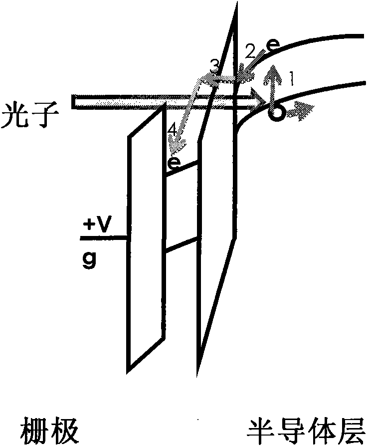
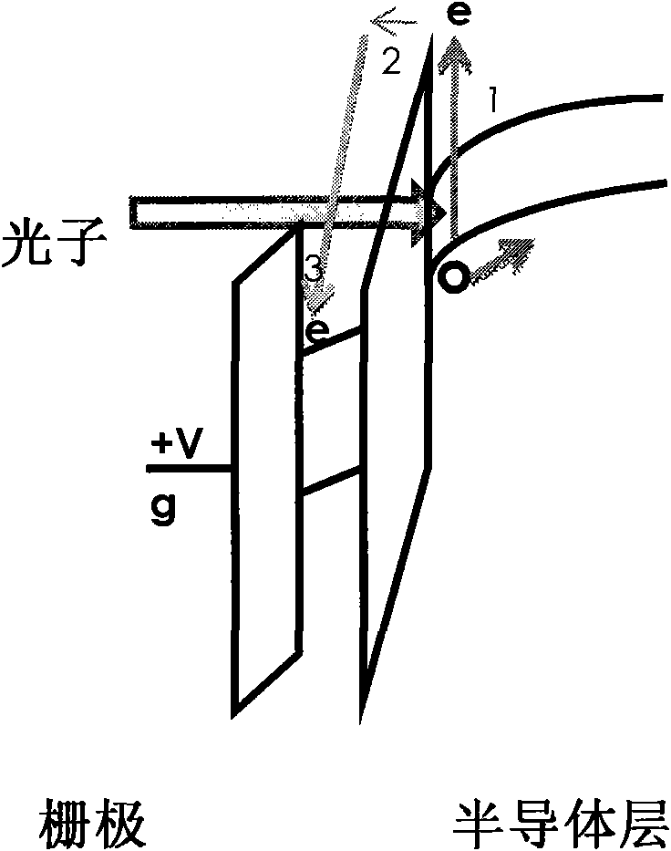
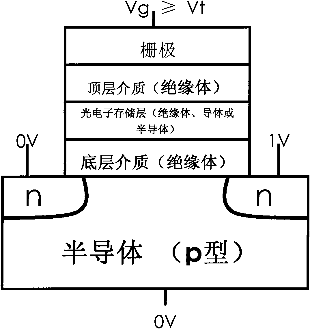
[0055] The working mechanism and process of the optoelectronic storage layer are as follows:

[0056] 1) Photoelectron collection and signal collection:

[0057] figure 1 , 2 Middle energy band diagram and photoelectron generation and migration diagram: Photoelectron generation in the figure 1. When hv>semiconductor Eg (or Eg+ΔEc), the photon is absorbed by the semiconductor, and an electron will be excited from the valence band to the conduction band;

[0058] 2. Photoelectron migration: When the voltage difference between the gate and the substrate is positive, photoelectrons migrate to the interface between the underlying medium and the semiconductor; when the voltage difference between the gate and the substrate is positive, if the photon hv>semiconductor Eg+semiconductor and the bottom layer The ΔEc of the medium, the excited photoelectrons will directly enter the photoelectron storage layer, migrate to the interface between the underlying medium and the semiconductor,...


PUM

PropertyMeasurementUnit
Thicknessaaaaaaaaaa

Abstract

The invention relates to an arrangement method of a photosensitive composite dielectric gate MOSFET (Metal-Oxide-Semiconductor Field Effect Transistor) detector. Each unit detector has a structure that N-shaped semiconductor regions are respectively arranged at both upper sides of a P-shaped semiconductor material of a substrate, two insulated dielectric material layers and a control grid electrode are respectively arranged over the substrate, a photoelectron storage layer is arranged between the two insulated dielectric material layers, the second insulated dielectric in contact with the control grid is made of a material preventing charges stored in the photoelectron storage layer from flowing into the grid electrode, a source electrode and a drain electrode are in suspended structures when photoelectrons are collected and stored to the photoelectron storage layer, the first insulated dielectric is a bottom dielectric and adopts silica, SiON or other dielectric materials with high dielectric constants, the second insulated dielectric layer is made from a top dielectric and adopts silica/silicon nitride/silica, silica, alumina or other dielectric materials with high dielectric constants, and the substrate layer or the grid electrode surface is provided with at least one transparent or semi-transparent window for detecting the wavelength of the detector.

Description

1. Technical field [0001] The invention relates to an imaging detection device, especially the structure, working mechanism, setting and operation method of an imaging detection device in the infrared, visible light band to ultraviolet band. 2. Background technology [0002] The currently developed imaging detection devices are mainly CCD and CMOS-APS. The basic working principle of CCD devices is related to the physical mechanism of metal-oxide-silicon (MOS) capacitors. The basic unit of CCD is MOS capacitors, and its working process is mainly signal Charge generation, storage, transfer and detection. CCD is a device that stores and transfers signals in the form of charge packets. Its outstanding feature is that it uses charges as signals, which is different from other devices that use current or voltage as signals. When the CCD is working, the clock pulse voltage is used to generate and control the change of the semiconductor potential well, thereby realizing the storage ...

Claims


Application Information

Patent Timeline
IPC IPC(8): H01L21/8234H01L27/14
Inventor 阎锋张荣施毅
Owner NANJING UNIV
Why Eureka
Try Eureka