Amorphous silicon solar cell with three-dimensional photonic crystal serving as back reflecting layer and manufacturing method thereof

A back reflective layer and photonic crystal technology, applied in photovoltaic power generation, circuits, electrical components, etc., can solve the problems of low reflectivity of the back reflective layer and low efficiency of amorphous silicon solar cells, so as to improve photon utilization efficiency and increase light Current density and photoelectric conversion efficiency, the effect of increasing the optical path of propagation

Inactive Publication Date: 2010-08-18
HARBIN INST OF TECH
View PDF5 Cites 17 Cited by
  • Summary
  • Abstract
  • Description
  • Claims
  • Application Information

AI Technical Summary

Problems solved by technology

[0006] The purpose of the present invention is to solve the problem that the low reflectivity of the existing Al back reflector leads to the low efficiency of the amorphous

Method used


Image

  • Amorphous silicon solar cell with three-dimensional photonic crystal serving as back reflecting layer and manufacturing method thereof
  • Amorphous silicon solar cell with three-dimensional photonic crystal serving as back reflecting layer and manufacturing method thereof
  • Amorphous silicon solar cell with three-dimensional photonic crystal serving as back reflecting layer and manufacturing method thereof

Examples


specific Embodiment approach 1

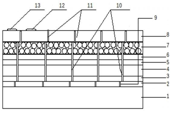
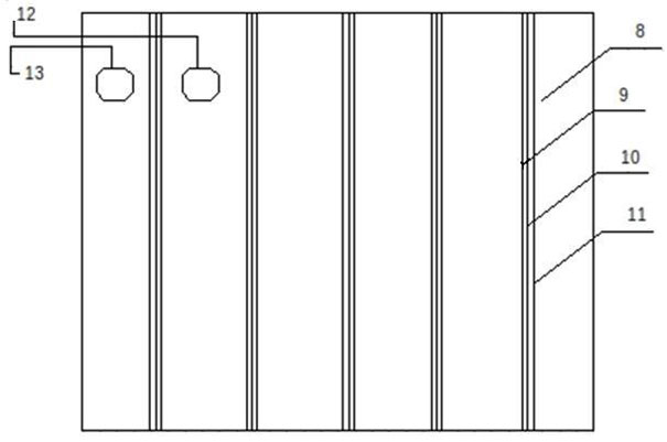
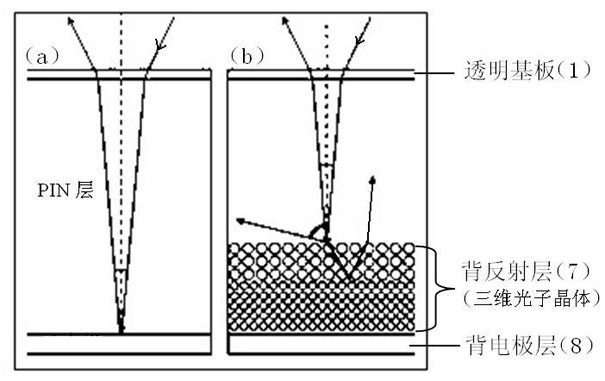
[0020] Specific Embodiment 1: In this embodiment, the three-dimensional photonic crystal is an amorphous silicon solar cell with a back reflection layer, including a front electrode layer 2, a P-SiC thin film layer 3, and an I-a-Si:H thin film layer stacked sequentially on a transparent substrate 1 4. N-a-Si:H film layer 5, back reflection layer 7, back electrode layer 8, first laser scribe line 9, second laser scribe line 10, mask wire 11, cathode wiring 12 and anode wiring 13, The amorphous silicon solar cell in which the three-dimensional photonic crystal is the back reflection layer also includes an ITO transparent conductive film 6, the back reflection layer 7 is a three-dimensional large-pore ordered aluminum-doped zinc oxide (AZO) film photonic crystal, and the ITO transparent conductive film 6 is located Between the back reflection layer 7 and the n-a-Si:H film layer 5.

[0021]In this embodiment, the amorphous silicon solar cells whose three-dimensional photonic cryst...

specific Embodiment approach 2

[0026] Embodiment 2: This embodiment differs from Embodiment 1 in that the thickness of the aluminum-doped zinc oxide thin film of the back reflection layer 7 is 0.5-1.5 μm, and the sheet resistance is 20-25 ohms / square. Other parameters are the same as in the first embodiment.

[0027] The back reflection layer of this embodiment is a three-dimensional photonic crystal, which can achieve omni-directional total reflection, and control the square resistance to 20-25 ohms / square, so as to achieve the purpose of reducing the series resistance as much as possible.

specific Embodiment approach 3

[0028] Embodiment 3: This embodiment differs from Embodiment 1 or Embodiment 2 in that the sheet resistance of the ITO transparent conductive film 6 is 5-10 ohms / square. Other parameters are the same as those in Embodiment 1 or Embodiment 2.

[0029] In this embodiment, the thickness of the ITO transparent conductive film 6 is 10-1000 nm, and the transmittance is greater than 80% in the wavelength range of 600 nm, which has no influence on the wavelength absorption and reflection of the solar cell.


PUM

PropertyMeasurementUnit
Thicknessaaaaaaaaaa
Particle sizeaaaaaaaaaa
Thicknessaaaaaaaaaa

Abstract

The invention discloses an amorphous silicon solar cell with a three-dimensional photonic crystal serving as a back reflecting layer and a manufacturing method thereof, relates to the method for manufacturing the amorphous silicon solar cell and solves the problem of low efficiency of the solar cell caused by low reflectivity of the traditional A1 back reflecting layer. The back reflecting layer of the amorphous silicon solar cell is a three-dimensional macroporous sequential aluminum-doped zinc oxide photonic crystal. The manufacturing method comprises the following steps: depositing a front electrode layer by low-pressure chemical vapor deposition, depositing a P-I-N layer by PECVD, preparing an ITO transparent conductive film by magnetron sputtering, preparing a colloidal crystal template by a vertical deposition process or spin-coating process, performing electrodeposition to obtain the back reflecting layer, and performing vacuum evaporation on a back electrode layer to obtain the back reflecting layer. The AZO has high transmissivity for visual light and can realize over 80 percent transmissivity for 600 to 1,000nm visual optical band when combined with the bandgap effect of the three-dimensional photonic crystal. The three-dimensional photonic crystal has big reflecting angle, so transmission optical path of optical waves in an absorbing layer is increased; the utilization rate of photons is improved; and photocurrent density and photoelectric conversion efficiency are increased.

Description

technical field [0001] The invention relates to an amorphous silicon solar cell and a preparation method thereof. Background technique [0002] Energy crisis and environmental pollution are major issues facing mankind, and the development of new energy and renewable clean energy is one of the most influential technical fields in the 21st century. Solar energy is an inexhaustible and renewable clean energy, and the research and development of solar cells has become increasingly important. Compared with crystalline silicon solar cells, amorphous silicon thin-film solar cells have the following advantages. The manufacturing process is simple; the substrate temperature is low, the consumables are less, and it can be deposited on a cheap substrate, so the cost is low, and the integration process can be easily applied, further cut costs. Therefore, the amorphous silicon thin film solar cell is a promising solar cell and has been extensively studied. [0003] At present, the ...

Claims


Application Information

Patent Timeline
IPC IPC(8): H01L31/042H01L31/0232H01L31/20H01L31/0216
CPCY02E10/52Y02P70/50
Inventor 李垚詹耀辉赵九蓬张一
Owner HARBIN INST OF TECH
Why Eureka
Try Eureka