Method for preparing titanium dioxide ultraviolet photoelectric detector

An electrical detector, titanium dioxide technology, applied in circuits, electrical components, semiconductor devices, etc., can solve the problems of high responsivity, large dark current, high UV-visible suppression ratio, and achieve the effect of simple process, easy integration and industrialization

Inactive Publication Date: 2010-09-01
XIAMEN UNIV
View PDF3 Cites 35 Cited by
  • Summary
  • Abstract
  • Description
  • Claims
  • Application Information

AI Technical Summary

Problems solved by technology

[0005] The purpose of the present invention is to aim at existing TiO 2 In order to provide a titanium dioxide ultraviolet photodetector with the advantages of high responsivity, small dark current, and high UV-visible suppression ratio due to the shortcomings of ultraviolet light detectors such as large dark current and small UV-visible suppression ratio

Method used


Image

  • Method for preparing titanium dioxide ultraviolet photoelectric detector
  • Method for preparing titanium dioxide ultraviolet photoelectric detector
  • Method for preparing titanium dioxide ultraviolet photoelectric detector

Examples


Embodiment Construction

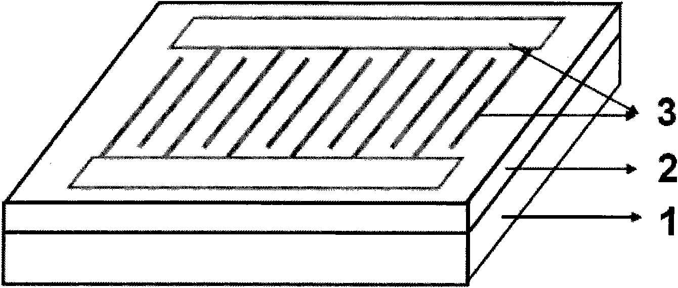
[0031] High-performance TiO prepared by the present invention 2 MSM-based UV photodetectors, interdigital electrode materials can be selected from metals with high work functions such as Au, Pt and Ni; insulating substrates can be selected from quartz glass, sapphire, and silicon wafers grown with silicon oxide or silicon nitride insulating layers . If it is made on a silicon wafer substrate, it can be compatible with the mature Si process, which is conducive to optoelectronic integration and easy to industrialize. The following uses quartz glass as the substrate and Au as the metal electrode to illustrate the preparation and implementation process of the detector of the present invention.

[0032] The specific steps are given below:

[0033] (1) Substrate treatment

[0034] Quartz glass (thickness 0.5mm, diameter 1inch) was selected as the insulating substrate, and the substrate was placed in toluene, acetone, ethanol and deionized water in sequence for ultrasonic cleaning...


PUM

PropertyMeasurementUnit
thicknessaaaaaaaaaa
particle sizeaaaaaaaaaa
thicknessaaaaaaaaaa

Abstract

The invention discloses a method for preparing a titanium dioxide ultraviolet photoelectric detector, relates to a semiconductor photoelectric detection device, and provides a titanium dioxide ultraviolet photoelectric detector with low dark current and a preparation method thereof. The detector has a metal-semiconductor-metal structure, and comprises an insulating substrate, a polycrystal TiO2 film deposited on the insulating substrate by using magnetron sputtering technology and an interdigital metal electrode prepared on the TiO2 film by using magnetron sputtering or electron beam evaporation technology from the bottom to the top. The high-quality polycrystal TiO2 film is deposited by adopting optimized sputtering process parameters, and the deposited film has ideal chemical proportion and high compactness and crystallinity. The MSM structural ultraviolet detector prepared by using the film as a matrix has the advantages of high response degree, low dark current, high ultraviolet visible suppression ratio and the like. The preparation method has simple process and low cost; if the detector is manufactured on a Si-based substrate, the method can be compatible with the mature Si process; and the method is favorable for photoelectric integration and easy for industrialization.

Description

technical field [0001] The invention relates to a semiconductor photodetection device, in particular to a polycrystalline TiO deposited by magnetron sputtering technology 2 MSM (metal-semiconductor-metal) structure ultraviolet photodetector with thin film as substrate and its preparation method. Background technique [0002] Ultraviolet detection technology has become another important photoelectric detection technology concerned by countries all over the world after infrared and laser detection technology, and has broad application prospects in scientific research, military, civil and many industrial fields. At present, the widely used ultraviolet photodetectors are mainly silicon-based ultraviolet phototubes and photomultiplier tubes. Their technology is mature and their sensitivity is high. Disadvantages such as additional filters. Wide bandgap semiconductor materials, such as SiC, GaN, ZnO and diamond film, have the characteristics of wide bandgap, high critical breakd...

Claims


Application Information

Patent Timeline
Patent Type & Authority Applications(China)
IPC IPC(8): H01L31/09H01L31/0224H01L31/18C23C14/35
CPCY02P70/50
Inventor 吴正云黄火林
Owner XIAMEN UNIV
Why Eureka
Try Eureka