

Silicon wafer rapid heat treatment phosphorus diffusion gettering technology for manufacture of solar cell
A rapid heat treatment, solar cell technology, applied in sustainable manufacturing/processing, final product manufacturing, circuits, etc., can solve the problem of low photoelectric conversion efficiency of silicon wafers, and achieve the goal of promoting the dissolution and diffusion of impurities, promoting gettering, and improving productivity. Effect
- Summary
- Abstract
- Description
- Claims
- Application Information
AI Technical Summary
Problems solved by technology
Method used
Image

Examples
Embodiment 1
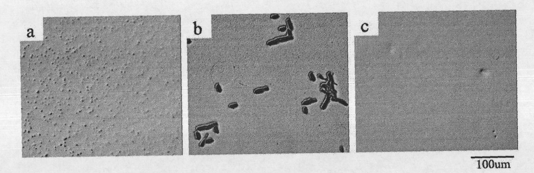
[0027] (1) Take a single crystal silicon wafer contaminated by Cu impurities, such as figure 2 As shown in (a), the body contains point-like copper precipitation, and the minority carrier lifetime is about 3 μs after testing;
[0028] (2) Coat the phosphorus source (p-854, Honeywell) on both sides of the monocrystalline silicon wafer, and then pre-bake it at 200°C for 10 minutes to remove excess organic matter;
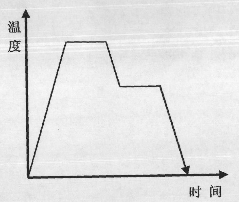
[0029] (3) Pass the protective gas (argon gas) into the RTP-300 rapid heat treatment furnace, the air pressure is about 1 atmosphere, and the above-mentioned single crystal silicon wafer is sent into the furnace, and the furnace temperature is raised to 850°C at 50°C / s, and kept for 3 Minutes, then lower the temperature to 650°C at a rate of 50°C / s, and keep it warm for 3 minutes. In addition, take the same treated monocrystalline silicon wafer and keep it at 900°C for 3 minutes. Impurities diffuse from the material body to the surface gettering region;
[0030] (4...
Embodiment 2
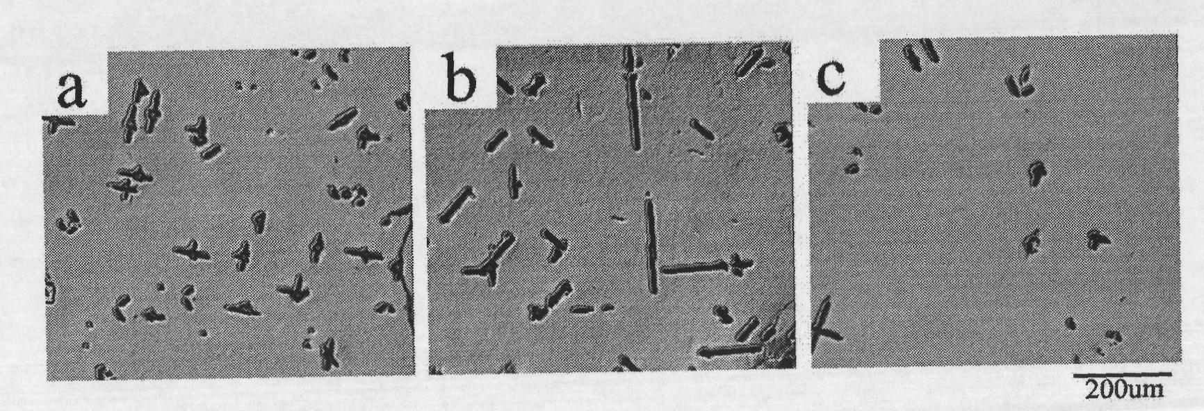
[0033] (1) Take a single crystal silicon wafer contaminated by Cu impurities, such as image 3 As shown in (a), the body contains star-shaped copper deposits, and the minority carrier lifetime is about 3 μs after detection;
[0034] (2) Coat the phosphorus source (p-854, Honeywell) on both sides of the monocrystalline silicon wafer, and then pre-bake it at 200°C for 10 minutes to remove the organic matter in the phosphorus source
[0035] (3) Pass the protective gas (argon gas) into the RTP-300 rapid heat treatment furnace, and the air pressure is about 1 atmosphere, and the above-mentioned single crystal silicon wafer is sent into the furnace. Minutes, then lower the temperature to 800°C at a rate of 30°C / s, and keep it warm for 3 minutes. In addition, take the same treated monocrystalline silicon wafer and keep it at 1000°C for 3 minutes, as a control group. Diffusion from the material body to the surface gettering region;
[0036] (4) Cool and remove the phosphosilicate g...
Embodiment 3
[0039] (1) Take a single crystal silicon wafer contaminated by Cu impurities, such as Figure 4 As shown in (a), the body contains star-shaped copper deposits, and the minority carrier lifetime is about 3 μs after detection;
[0040] (2) Coat the phosphorus source (p-854, Honeywell) on both sides of the monocrystalline silicon wafer, and then pre-bake it at 200°C for 10 minutes to remove excess organic matter;
[0041](3) Pass the protective gas (oxygen) into the RTP-300 rapid heat treatment furnace, the air pressure is about 1 atmosphere, and the above-mentioned single crystal silicon wafer is sent into the furnace, and the furnace temperature is raised to 950°C at 200°C / s, and kept for 3 minutes , and then lower the temperature to 700°C at a rate of 10°C / s, and hold for 3 minutes. The holding time selected in the experiment is enough for Cu impurities to diffuse from the material body to the surface gettering area;
[0042] (4) Cool and remove the phosphosilicate glass laye...
PUM
 Abstract
Description
Claims
Application Information