Semiconductor sensor and production method

A sensor and semiconductor technology, used in semiconductor devices, final product manufacturing, sustainable manufacturing/processing, etc., can solve problems such as long response and response time, cumbersome functional processes, and unfavorable large-scale applications, achieving low price, Effects of cost reduction, photoresponse and recovery time reduction

Inactive Publication Date: 2010-10-20
LANZHOU UNIVERSITY
View PDF5 Cites 24 Cited by
  • Summary
  • Abstract
  • Description
  • Claims
  • Application Information

AI Technical Summary

Problems solved by technology

First, the response current changes caused by photon irradiation are very small, requiring expensive instruments to detect tiny current signals
Secondly, after the photons irradiate the semiconductor, the response and recovery time is long, which makes the detection inconvenient
For the first difficulty, the current solution is roughly as follows. R.S.Aga.Jr et al. modified the surface of zinc oxide nanowires with CdTe quantum dots, which made the photoresponse curve roughly increased by less than 5nA. Although the photoresponse current has increased, but Probing currents at the nA level requires very expensive instruments, see R.S.Aga, Jr et.al, Appl.Phys.Lett.91, 232108 (2007)
J.H.He et al. functionalized the surface of ZnO nanobelts, and greatly increased the electrical signal intensity to 100 times that of the baseline. However, since the baseline is almost zero, the actual electrical signal after photon irradiation is still very weak, and the functional The process of chemicalization is cumbersome, which is not conducive to large-scale application, see J.H.He, J.Appl.Phys.102, 084303 (2007)

Method used


Image

  • Semiconductor sensor and production method
  • Semiconductor sensor and production method
  • Semiconductor sensor and production method

Examples


Embodiment 1

[0031] Embodiment 1: Detecting ultraviolet photons by using zinc oxide nanowire ultraviolet photon detectors with ohmic contacts of different integration levels.

[0032] 1. Preparation of ZnO nanowire arrays using a vacuum tube furnace

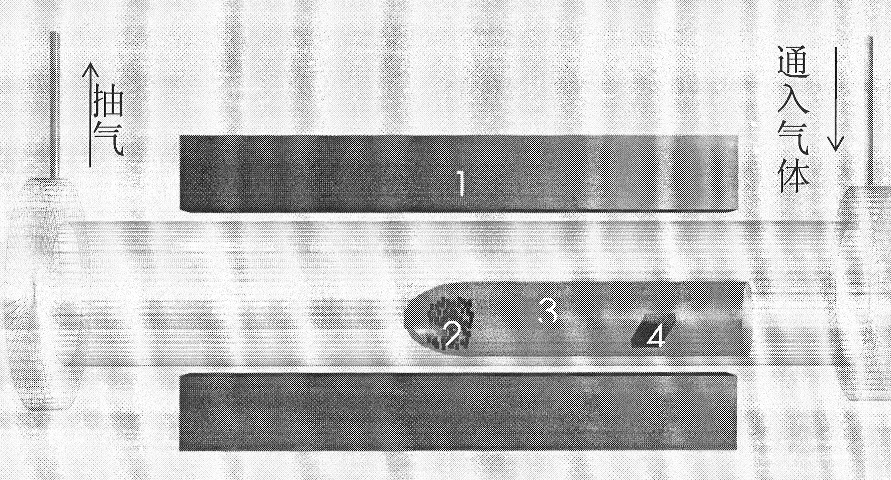
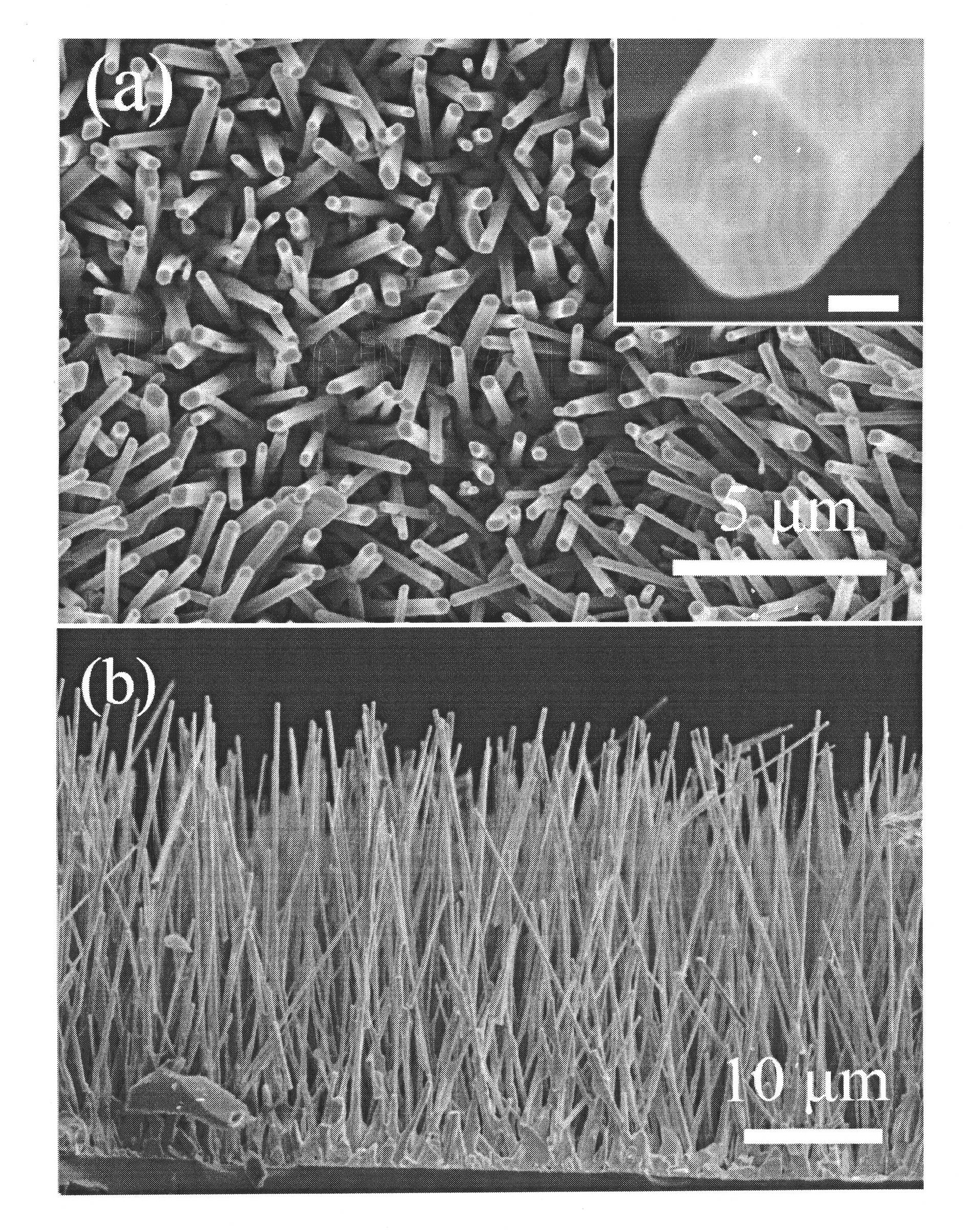
[0033] The vacuum tube furnace used in the embodiment of the present invention is referring to appendix figure 1 , figure 1 Middle: 1 is a tube furnace, 2 is a mixture of zinc oxide and carbon placed in a casing, 3 is a quartz casing, and 4 is a silicon substrate. The outer diameter of the tube furnace used in the present invention is 60 centimeters, and the length is 100 cm, and the outer diameter of the single opening casing is 18 mm, and the length is 28 cm. The length of the constant temperature zone of the tube furnace is 20cm.

[0034] During preparation, put the ground mixture of 0.81g of zinc oxide and 0.12g of graphite powder into the reaction boat, and the reaction boat is put into the closed end of the single-open casing. Cut t...

Embodiment 2

[0043] Implementation Example 2: Using a zinc oxide nanowire ultraviolet photon detector with Schottky contacts of different integration levels to detect ultraviolet photons.

[0044] 1. The preparation method of the zinc oxide nanowire array is as in Example 1.

[0045] 2. Preparation of Schottky contact ZnO nanowire UV photon detector.

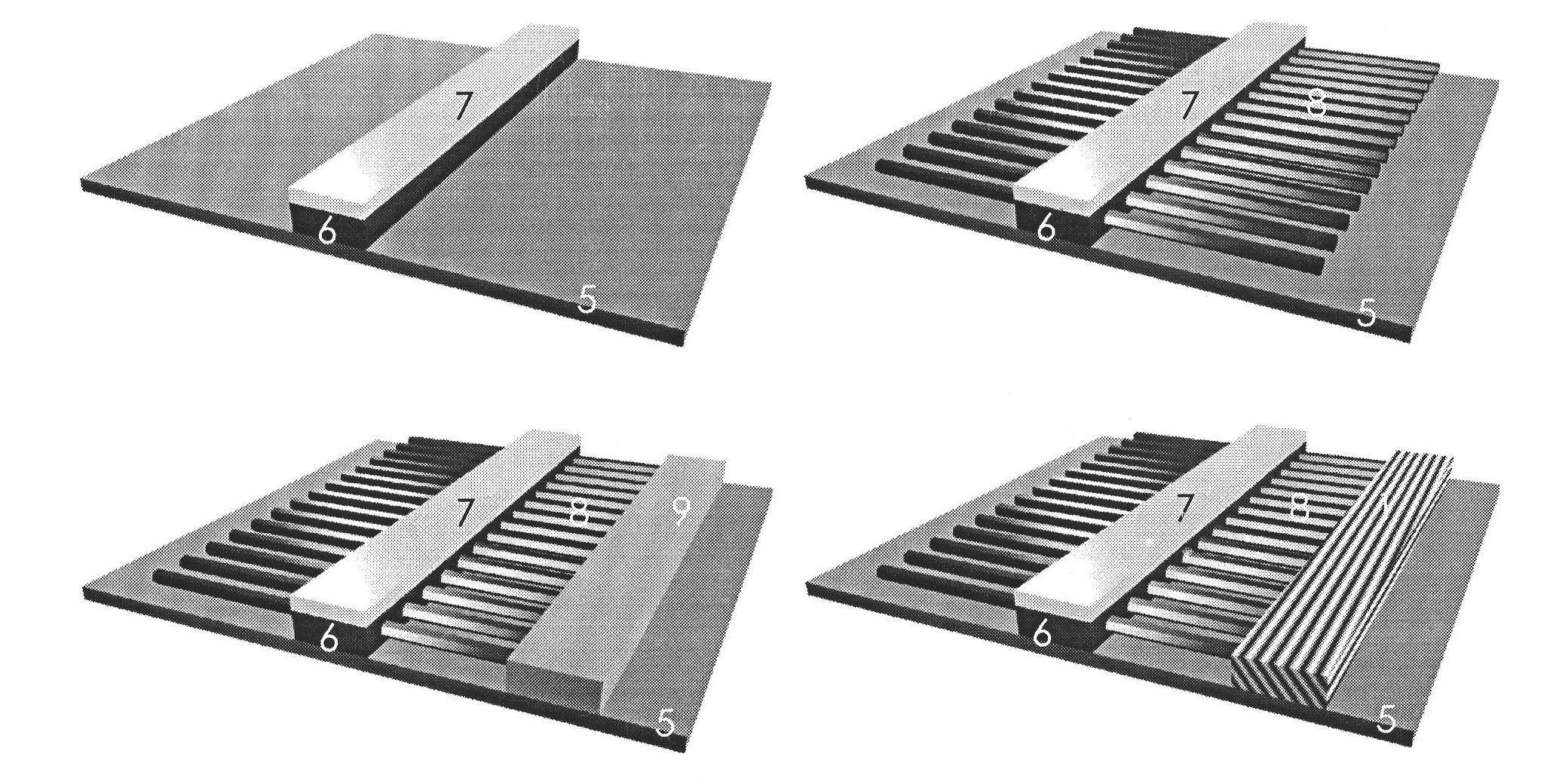
[0046] After cleaning and drying the other piece of glass, place the silicon wafer product facing the glass piece, and apply a certain amount of positive pressure to slide the silicon piece over the surface of the glass piece in the same direction. The nanowires on the glass sheet and almost parallel to each other are spin-coated with a layer of photoresist on the glass sheet. The rotation speed of the spinner is from slow to fast, and the final rotation speed is 3000 rpm, and the rotation speed is maintained for 60 seconds. Then pre-baked in an oven at 90 degrees Celsius for 40 minutes, and then under the microscope of the photolithography...

Embodiment 3

[0049] Implementation Example 3: Using a Schottky-contacted zinc oxide nanowire ultraviolet photon detector to detect ultraviolet photons of different intensities, different photon response curves are obtained from different photon intensities.

[0050] 1. The preparation method of the zinc oxide nanowire array is as in Example 1.

[0051] 2. Prepare a Schottky contact ultraviolet photon detector as in Example 2.

[0052] 3. Device testing

[0053] The intensity of ultraviolet photons irradiated on the detector is changed from 0.1μw / cm 2 to 3000μw / cm 2 Changes, the photoresponse current ranging from 0.2nA to 6μA and corresponding to the intensity is obtained. For specific tests, see the attached Figure 8 with 9 .

[0054] UV sensor composed of seven nanowires tested 22-3000μW / cm 2 The photoresponse current curves under different ultraviolet light intensities are shown in the appendix Figure 8 , starting from the curve closest to the abscissa, the measured UV photon inte...


PUM


Abstract

The invention discloses a sensor for ultraviolet detection and a production method thereof. The semiconductor sensor of the invention is integrated by two electrodes, and a zinc oxide nanowire positioned between the two electrodes in a parallel way. The production method of the semiconductor sensor of the invention comprises the following steps of: firstly growing a layer of zinc oxide nanowire array which is vertical to a substrate surface on a first substrate, then transferring the zinc oxide nanowire array onto the surface of a second substrate, placing an electrode pattern on a masking film plate onto a gluing surface, making the electrode pattern be vertical to the two ends of the oriented nanowire and cover the end parts of the nanowire so as to carry out exposing, developing and photoetching, then depositing at least one electric conduction metal-made electrode in an electrode area which is formed by photoetching in a physical method, then stripping the electrodes and the nanowire from the second substrate, connecting leads onto the electrodes, and finally obtaining the required device.

Description

technical field [0001] The invention relates to a semiconductor sensor and a preparation method of the device. The semiconductor sensor described in the present invention refers to a sensor for ultraviolet detection. Background technique [0002] Ultraviolet detection is a new detection technology developed after infrared detection and laser detection, and has very broad application prospects in both military and civilian fields. In terms of military use, in the late 1980s, military research on ultraviolet technology has begun abroad, and certain progress has been made. The U.S. Navy’s C-130S helicopter and P-3S transport plane have the world’s first ultraviolet warning device AAR-47, and it was put into actual combat in the Gulf War in 1991. At present, the U.S. military is actively funding the development of new ultraviolet detectors. Only Magnolia Optical Technology Company has received 1.25 million US dollars of funding for research in this area, see Kebian, "Aerospace...

Claims


Application Information

Patent Timeline
Patent Type & Authority Applications(China)
IPC IPC(8): H01L31/09H01L31/0352H01L31/18
CPCY02P70/50
Inventor 秦勇吴巍炜白所崔暖洋
Owner LANZHOU UNIVERSITY
Why Eureka
Try Eureka