

Growing method of high-crystal quality high-resistance GaN epitaxial layer
A growth method and epitaxial growth technology, which are applied in the field of growing high-resistance GaN epitaxial layers, can solve problems affecting device performance, high dislocation density of high-resistance GaN epitaxial layers, strong electron scattering, etc., to increase stability and reliability, The effect of reducing the content of oxygen impurities and increasing the degree of freedom
- Summary
- Abstract
- Description
- Claims
- Application Information
AI Technical Summary
Problems solved by technology
Method used
Image

Examples
Embodiment 1
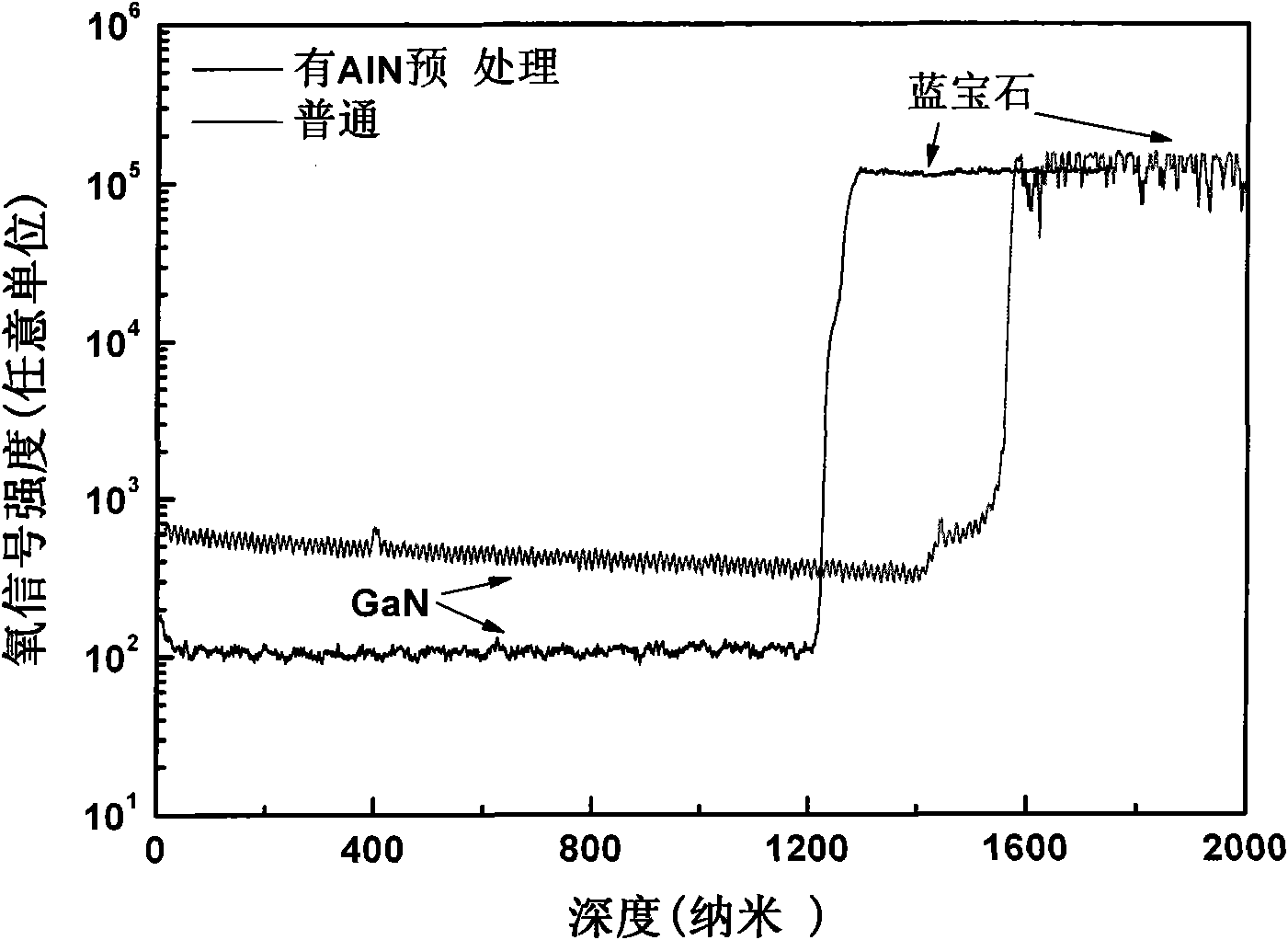
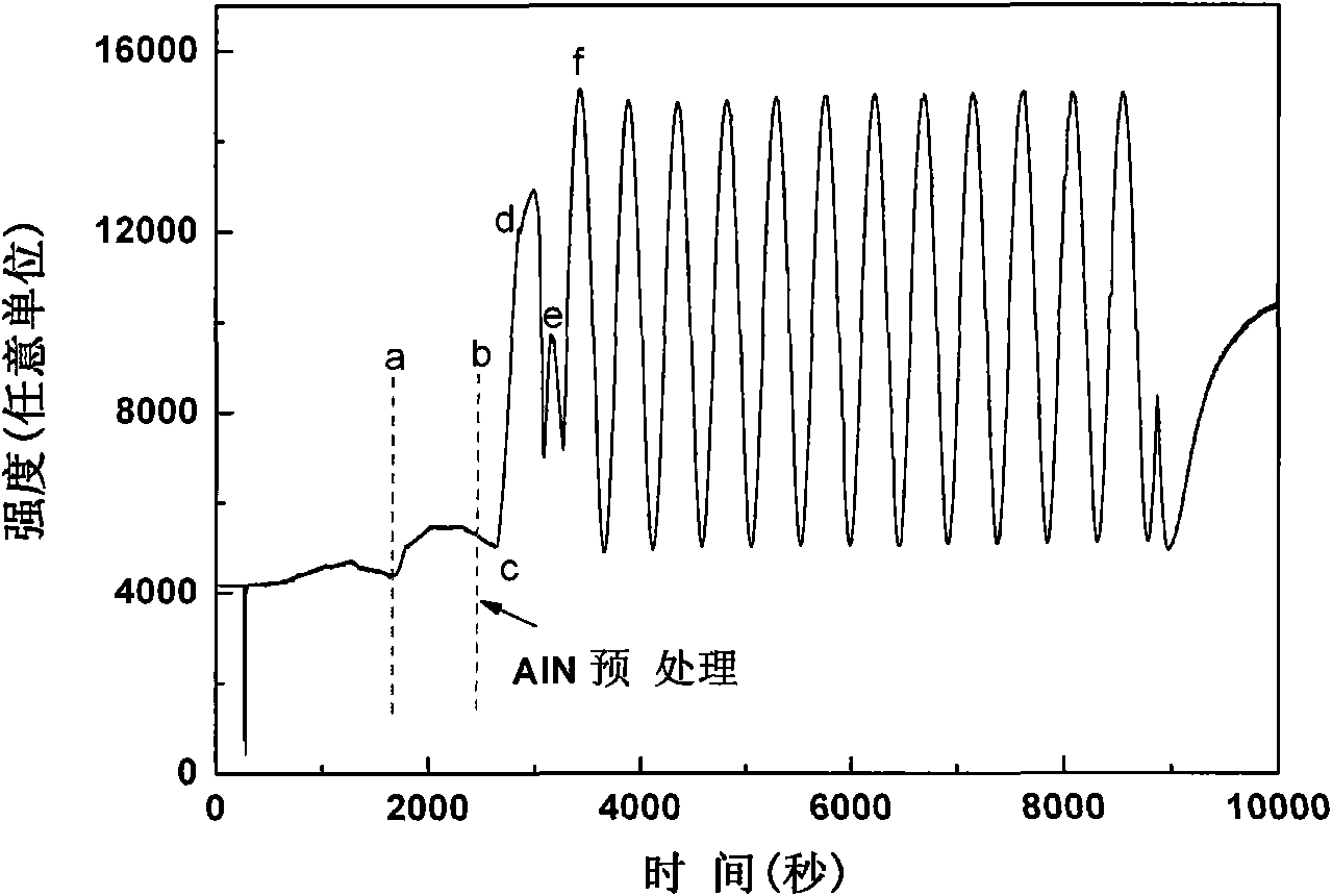
[0040] For the growth of GaN epitaxial layer with high crystal quality and high resistance, 3 batches of samples were prepared according to the following conditions, showing the optimization process of "AlN pretreatment". In addition, 1 batch of samples was prepared according to the conventional conditions (ie, the following 2) and 3) steps were omitted):
[0041] 1) Use MOCVD equipment (3×2”Thomas Swan Close Coupled Showerhead MOCVD), the substrate is a sapphire substrate on the (0001) plane, and the H 2 , the reaction chamber pressure is 300Torr, bake at 1090°C for 5min, and clean the substrate;
[0042] 2) Cool down to 630°C, feed trimethylaluminum and ammonia gas, H 2 as a carrier gas. The reaction chamber pressure is 60Torr, low-temperature AlN is grown, and the growth thicknesses are 10, 16, and 28nm respectively.
[0043] 3) Keep the pressure of the reaction chamber at 60 Torr, stop feeding trimethylaluminum, continue feeding ammonia gas, raise the temperature to 1100...
Embodiment 2
[0053] High crystal quality and high resistance GaN epitaxial layer growth, keeping the AlN growth conditions unchanged, changing the AlN annealing time, and preparing two furnace samples:
[0054] 1) Use MOCVD equipment (3×2”Thomas Swan Close Coupled Showerhead MOCVD), the substrate is a sapphire substrate on the (0001) plane, and the H 2 , the reaction chamber pressure is 300Torr, bake at 1090°C for 5min, and clean the substrate;
[0055] 2) Cool down to 680°C, feed trimethylaluminum and ammonia, H 2 as a carrier gas. The pressure of the reaction chamber is 75 Torr, the low-temperature AlN is grown, and the growth thickness is 25 nm.
[0056] 3) Stop feeding trimethylaluminum, continue feeding ammonia gas, adjust the pressure of the reaction chamber to 100 Torr, raise the temperature to 1110° C. in 240 seconds, and set the annealing time to 100 and 800 seconds respectively.
[0057] 4) Cool down to 530°C, feed trimethylgallium and ammonia gas, H 2 as a carrier gas. The ...
PUM
| Property | Measurement | Unit |
|---|---|---|
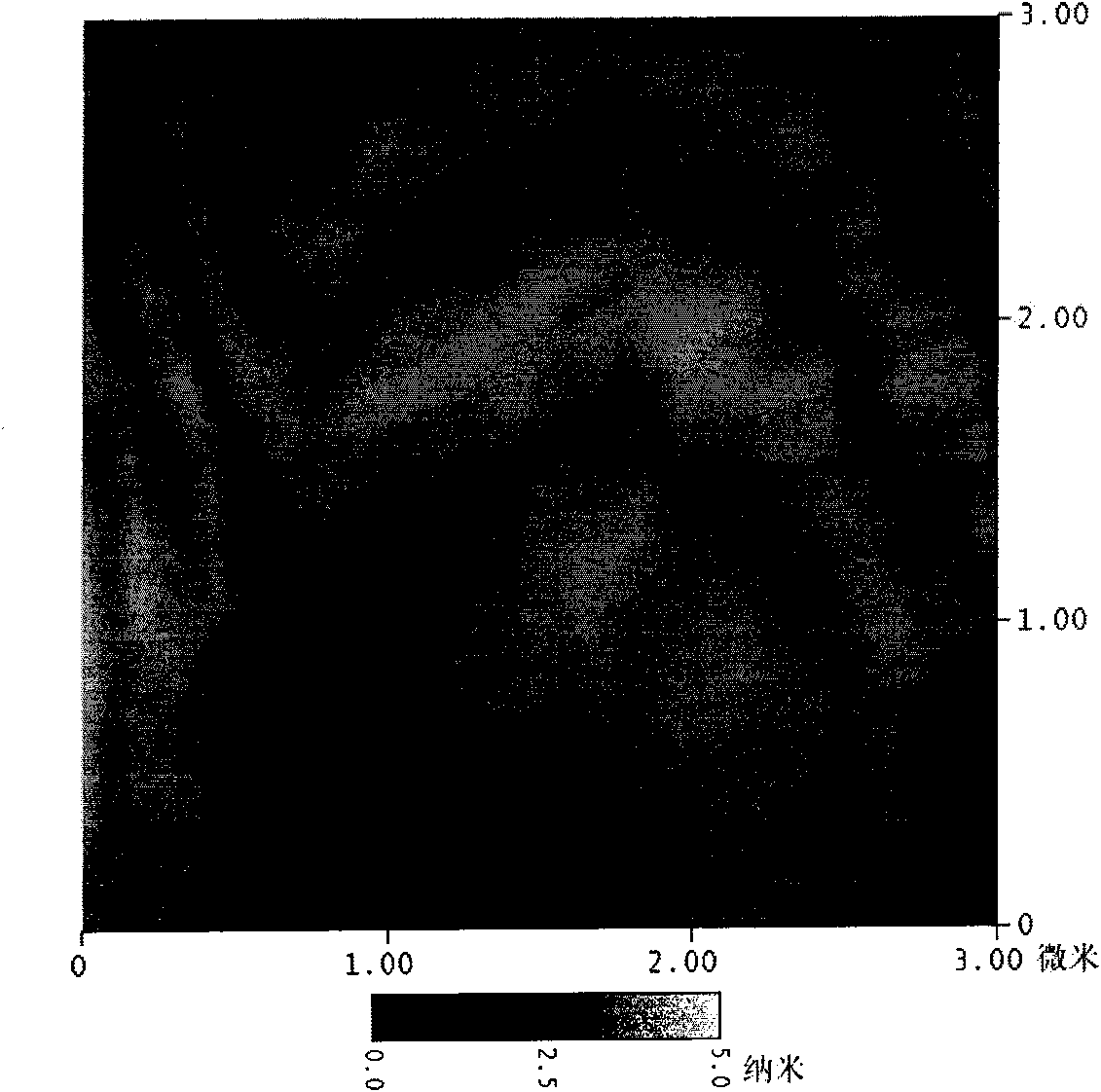
| Sheet resistance | aaaaa | aaaaa |
| Surface roughness | aaaaa | aaaaa |
Abstract
Description
Claims
Application Information