Electric conductivity adjustable organic molecular film and semiconductor hybrid material and preparation method thereof

A technology of organic molecules and conductive properties, applied in the field of preparation of organic molecular films and semiconductor hybrid materials

Inactive Publication Date: 2010-11-24
INST OF CHEM CHINESE ACAD OF SCI
View PDF0 Cites 6 Cited by
  • Summary
  • Abstract
  • Description
  • Claims
  • Application Information

AI Technical Summary

Problems solved by technology

[0005] The purpose of the present invention is to improve the conductivity of semiconductor materials, doping organic molecules with optical switching functions and inorganic semiconductor (such as single crystal silicon semiconductor) materials to obtain organic molecular films with adjustable conductivity and semiconductor hybridization. materials, so as to realize the intelligent control of the electrical conductivity of the hybrid material; at the same time, it can be uniformly doped in the semiconductor material in the nanometer range with organic molecules and inorganic semiconductor materials that have the function of optical switching, avoiding the inadequacy caused by the doping of inorganic elements. Uniformity causes defects such as voids in semiconductor materials

Method used


Image

  • Electric conductivity adjustable organic molecular film and semiconductor hybrid material and preparation method thereof
  • Electric conductivity adjustable organic molecular film and semiconductor hybrid material and preparation method thereof
  • Electric conductivity adjustable organic molecular film and semiconductor hybrid material and preparation method thereof

Examples


Embodiment 1

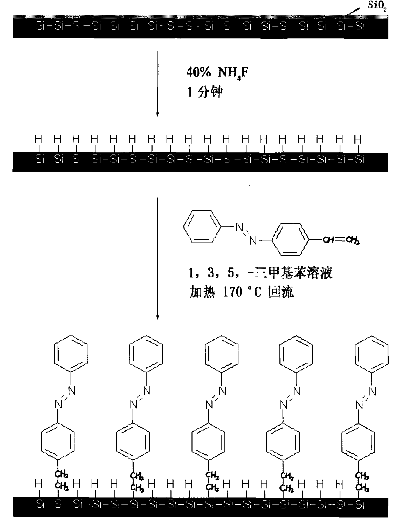
[0074] (1) Cleaning of the monocrystalline silicon semiconductor substrate: the monocrystalline silicon semiconductor substrate with the crystal form being (111) was cleaned successively with acetone and methane for 15 minutes; then placed in concentrated sulfuric acid with a mass concentration of 98% and In a mixture of 30% hydrogen peroxide, keep it at a temperature of 90°C for 50 minutes, take it out and use a resistivity > 18MΩcm -1 Fully cleaned with ultrapure water, wherein the volume ratio of concentrated sulfuric acid with a mass concentration of 98% and hydrogen peroxide with a mass concentration of 30% is 3:1;

[0075] (2) Pretreatment of the monocrystalline silicon semiconductor substrate: soak the cleaned monocrystalline silicon semiconductor substrate of the crystal type (111) obtained in step (1) in an aqueous ammonium fluoride solution with a mass concentration of 30% for 60 seconds to remove The oxide layer of the monocrystalline silicon semiconductor substrate...

Embodiment 2

[0086] (1) Cleaning of the monocrystalline silicon semiconductor substrate: the monocrystalline silicon semiconductor substrate with the crystal form being (100) was cleaned successively with acetone and methane for 15 minutes; In a mixture of 30% hydrogen peroxide, keep it at 100°C for 40 minutes, take it out and use a resistivity > 18MΩcm -1 Fully cleaned with ultrapure water, wherein the volume ratio of concentrated sulfuric acid with a mass concentration of 98% and hydrogen peroxide with a mass concentration of 30% is 3:1;

[0087] (2) Pretreatment of the monocrystalline silicon semiconductor substrate: soaking the cleaned monocrystalline silicon semiconductor substrate of crystal type (100) obtained in step (1) in 1% hydrofluoric acid aqueous solution for 2 minutes to remove The oxide layer of the monocrystalline silicon semiconductor substrate; the prepared substrate is placed in an oxygen-free environment and sealed for storage;

[0088] (3) Configure an organic molecu...

Embodiment 3

[0098](1) Cleaning of the monocrystalline silicon semiconductor substrate: the monocrystalline silicon semiconductor substrate with the crystal form being (111) was cleaned successively with acetone and methane for 15 minutes; then placed in concentrated sulfuric acid with a mass concentration of 98% and In a mixture of 30% hydrogen peroxide, keep it at a temperature of 90°C for 55 minutes, take it out and use a resistivity > 18MΩcm -1 Fully cleaned with ultrapure water, wherein the volume ratio of concentrated sulfuric acid with a mass concentration of 98% and hydrogen peroxide with a mass concentration of 30% is 3:1;

[0099] (2) Pretreatment of the monocrystalline silicon semiconductor substrate: soaking the cleaned monocrystalline silicon semiconductor substrate of the crystal type (111) obtained in step (1) in an aqueous ammonium fluoride solution with a mass concentration of 15% for 90 seconds to remove The oxide layer of the monocrystalline silicon semiconductor substra...


PUM


Abstract

The invention relates to electric conductivity adjustable organic molecular film and semiconductor hybrid material and a preparation method thereof. The preparation method comprises the following steps of: placing a cleaned monocrystalline silicon semiconductor substrate of which an oxidation layer is removed into 1,3,5-trimethylbenzene solvent in which organic molecules are dissolved in a closed quartz container; removing oxygen of the 1,3,5-trimethylbenzene solvent in which the organic molecules are dissolved by using high-purity argon gas or nitrogen gas; and modifying the organic molecules into a polishing surface of the monocrystalline silicon semiconductor substrate by illuminating the closed container or refluxing the 1,3,5-trimethylbenzene solvent in which the organic molecules are dissolved to obtain the electric conductivity adjustable organic molecular film and semiconductor hybrid material. The electric conductivity adjustable organic molecular film and semiconductor hybrid material is characterized in that a monomolecular film of organic molecule with light switch function is modified on the polished surface of the monocrystalline silicon semiconductor substrate. The doping uniformity of the organic molecules in the integral and nanometer range can be met, and the adjustment of the electric conductivity adjustable organic molecular film and semiconductor hybrid material by light with specific wavelength can be realized.

Description

technical field [0001] The invention belongs to the field of intelligent semiconductor materials, and in particular relates to an organic molecular film with adjustable conductivity and a semiconductor hybrid material obtained by chemically modifying the surface of a semiconductor, and a preparation method for an organic molecular film with adjustable conductivity and a semiconductor hybrid material . Background technique [0002] At present, the electronics industry is the largest industry in the world and a pillar industry in many developed countries. Semiconductor devices are the foundation of the electronics industry. It is of great significance to study and improve the performance of semiconductors. [0003] At present, the modification method of semiconductor materials is mainly to use artificial doping method in semiconductor materials to dope inorganic materials in semiconductor materials (such as doping boron or phosphorus in silicon), or by changing the structural ...

Claims


Application Information

Patent Timeline
Patent Type & Authority Applications(China)
IPC IPC(8): H01L51/30H01L51/40C07C245/08C07D491/107C07D409/14C07D333/36C07D409/06C07D307/62C07D207/42
Inventor 张兴业温永强宋延林
Owner INST OF CHEM CHINESE ACAD OF SCI
Why Eureka
Try Eureka