Method for preparing organic light-emitting diode (OLED) display screen by full printing process

A technology of electroluminescence and display screen, applied in circuits, electrical components, electrical solid devices, etc., to achieve the effect of good affinity and easy processing

Active Publication Date: 2010-12-15
SOUTH CHINA UNIV OF TECH
View PDF5 Cites 41 Cited by
  • Summary
  • Abstract
  • Description
  • Claims
  • Application Information

AI Technical Summary

Problems solved by technology

However, solution processing and printing of the OLED back

Method used


Image

  • Method for preparing organic light-emitting diode (OLED) display screen by full printing process
  • Method for preparing organic light-emitting diode (OLED) display screen by full printing process
  • Method for preparing organic light-emitting diode (OLED) display screen by full printing process

Examples


Embodiment 1

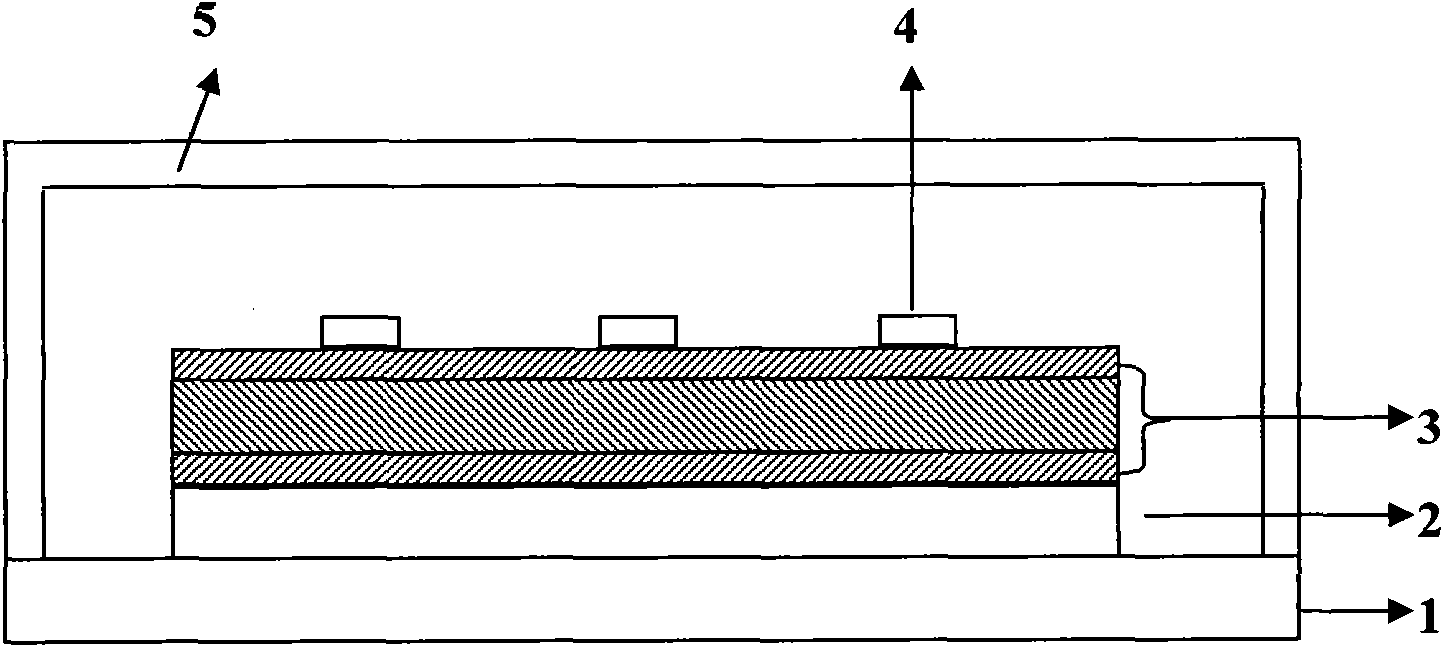
[0024] Such as figure 1 As shown, an organic electroluminescence display device is composed of a substrate 1 , a substrate electrode 2 , an organic functional layer 3 and a back electrode 4 sequentially stacked. The substrate 1 is a hard substrate or a flexible substrate; the substrate electrode is a transparent or translucent opaque anode, and the organic functional layer 3 includes at least a light emitting layer. Substrate (including electrodes) preparation: commercially available ITO transparent conductive glass with a pixel structure is used as the substrate 1 and the substrate electrode 2 .

[0025] Preparation of organic functional layer 3: PEDOT:PSS aqueous solution (polyaniline derivative, model 4083, purchased from Bayer, Germany) was poured on the cleaned ITO glass, and the hole injection layer was prepared by spin coating (also used as the anode Buffer layer) (film thickness 40nm at 2600rpm), and then moved into a nitrogen glove box (model NEXUS, produced by VAC, ...

Embodiment 2

[0035] Substrate (including electrodes) preparation: a commercially available ITO transparent polyethylene terephthalate (PET) film with a pixel structure is used as a substrate, which is a flexible substrate.

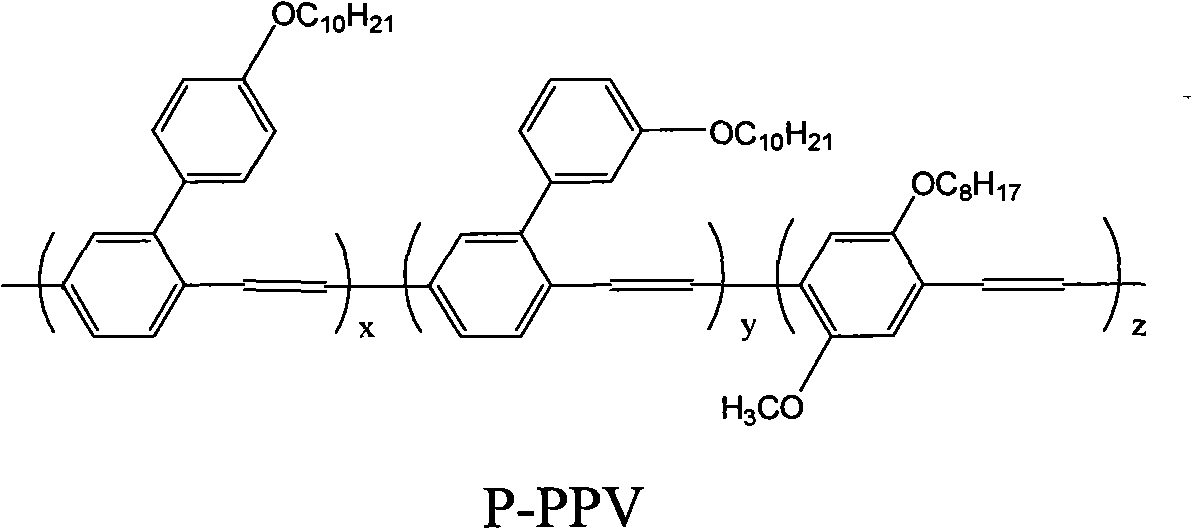
[0036] Preparation of organic functional layer: PEO (polyethylene oxide, molecular weight ~ 1 million, purchased from Sigma-Aldrich, USA) was dissolved in water (concentration 16 mg / ml), and PEDOT:PSS (polyaniline derivative, model 4083, (purchased from Bayer, Germany) were blended at a volume ratio of 3:2, and the hole injection layer (also used as an anode buffer layer) was prepared by screen printing (screen size 300 mesh, film formation 40-50nm). Then move into a nitrogen glove box (model NEXUS, produced by VAC Company of the United States). Heat on a hot stage at 200°C for 10 minutes. Select a high luminous efficiency green light material, a poly(phenylphenylene vinylene) derivative P-PPV, with a molecular weight of 150,000 to 300,000. The molecular structural f...

Embodiment 3

[0044] Substrate (including electrodes) preparation: commercially available IZO transparent conductive quartz with a pixel structure is used as the substrate.

[0045] Preparation of organic functional layer: PEDOT:PSS (polyaniline derivative, model 4083, purchased from Bayer, Germany) was poured on the cleaned IZO quartz, and hole injection was prepared by spin coating method (film thickness 40nm at 2600rpm) layer (also as an anode buffer layer), and then moved into a nitrogen glove box (model NEXUS, produced by VAC Corporation of the United States). Heat on a hot stage at 200°C for 10 minutes. The hole transport material PVK (polyvinylcarbazole, Sigma-Aldrich, USA) was dissolved in chlorobenzene solvent (concentration ~ 10 mg / ml). After being fully dissolved, the solution was poured on the hole injection layer, and a hole transport layer was prepared by a spin coating method (with a film thickness of 40 nm at 2000 rpm). Select high-efficiency blue light material: dendrimer...


PUM


Abstract

The invention relates to a method for preparing an OLED display screen by a full printing process. The OLED display screen is formed by sequentially laminating a substrate, a substrate electrode, organic functional layers and a back electrode, wherein the substrate is made of a hard substrate or a soft substrate; the substrate electrode is a transparent or semi-transparent anode; the organic functional layers at least comprise light-emitting layers; the back electrode is prepared into a cathode by a printing process; the organic functional layers are prepared by performing rotary coating, ink-jet printing, screen printing, pulling and spraying on non-polar organic light-emitting polymers, small molecules or tree-like compounds on the substrate electrode. The method can completely simply the manufacturing process of full-color OLED display screens, further reduce the equipment requirement and manufacturing cost, greatly promote the solution for the high cost problem of the conventional OLEDs, and especially provide a brand-new technical scheme for manufacturing large-area OLED display screens without using an expensive and time-wasting vacuum vapor deposition system.

Description

technical field [0001] The invention relates to an electroluminescence display screen, in particular to a process for preparing an organic electroluminescence display screen by realizing a full printing method. Background technique [0002] Organic electroluminescent technology (OLED) is a new generation of display technology. Compared with the current mainstream liquid crystal display technology, it has ultra-thin, active light, high brightness, high contrast, wide viewing angle, fast response, high luminous efficiency, and temperature adaptability. Good performance, simple production process, low driving voltage, low energy consumption, bendable and foldable, etc., have attracted extensive attention from the industry, and are considered to be one of the most competitive new generation flat panel display technologies research hotspot. OLED displays can be widely used in the display of electronic equipment such as mobile phones, digital cameras, notebook computers, and tele...

Claims


Application Information

Patent Timeline
IPC IPC(8): H01L51/56H01L27/32
Inventor 郑华曹镛彭俊彪王坚汪青郑奕娜陈海波张赤
Owner SOUTH CHINA UNIV OF TECH
Why Eureka
Try Eureka