

Method for improving photoelectric conversion efficiency of crystal silicon solar battery
A photoelectric conversion efficiency, solar cell technology, applied in the direction of circuits, electrical components, semiconductor devices, etc., can solve the problems that are not enough to make up for the increase in cost, the process is complicated, and it is difficult to apply to actual production. It is suitable for large-scale production and equipment. Low investment and the effect of improving photoelectric conversion efficiency
- Summary
- Abstract
- Description
- Claims
- Application Information
AI Technical Summary
Problems solved by technology
Method used
Image

Examples
Embodiment 1
[0027] 1. Perform acid texturing and pre-diffusion cleaning on P-type polysilicon wafers;
[0028] 2. Wafer in POCl 3 Diffusion of high-temperature phosphorus is carried out under the atmosphere, the entire diffusion surface is doped with low concentration, the sheet resistance is 60Ω / □, and POCl 3 Reacts with silicon to form phosphosilicate glass;
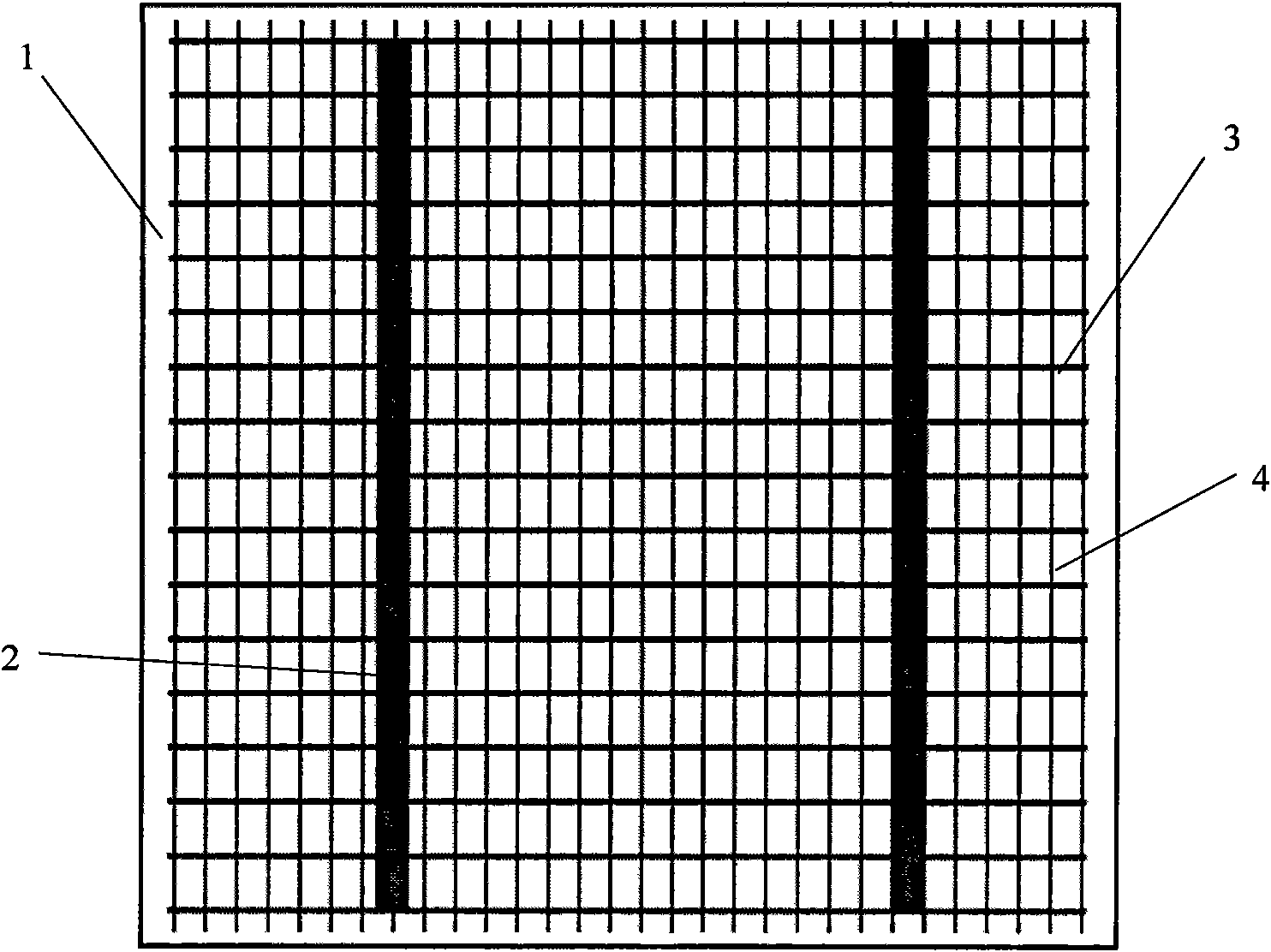
[0029] 3. If figure 1 As shown in the figure, a laser with a power of 10W and a wavelength of 532nm is used to scan parallel lines on the surface of a silicon wafer covered with phosphosilicate glass, so that the phosphorous in the phosphosilicate glass at the irradiated area diffuses into the silicon, forming a thin parallel line array doped with high concentration. , the distance between parallel lines is 2mm;
[0030] 4. Etch the edge of the silicon wafer to remove the peripheral PN junction;
[0031] 5. After washing away the phosphosilicate glass on the surface of the silicon wafer, deposit a silicon nitride anti-reflecti...
Embodiment 2
[0034] 1. Alkali texturing and pre-diffusion cleaning of P-type monocrystalline silicon wafers;
[0035] 2. Wafer in POCl 3 Diffusion of high-temperature phosphorus is carried out in the atmosphere, the entire diffusion surface is doped with low concentration, the sheet resistance is 120Ω / □, and POCl 3 Reacts with silicon to form phosphosilicate glass;
[0036] 3. If figure 1 As shown, use a laser with a power of 10W and a wavelength of 532nm to scan the surface of a silicon wafer covered with phosphosilicate glass, so that the phosphorous in the phosphosilicate glass at the irradiated area diffuses into the silicon, forming an array of highly doped thin parallel lines. The spacing is 0.3mm;
[0037] 4. Etch the edge of the silicon wafer to remove the peripheral PN junction;
[0038] 5. After washing away the phosphosilicate glass on the surface of the silicon wafer, deposit a silicon nitride anti-reflection film on the diffusion surface;
[0039] 6. Screen printing front...
Embodiment 3
[0041] 1. Alkali texturing and pre-diffusion cleaning of P-type monocrystalline silicon wafers;
[0042] 2. Wafer in POCl 3 Diffusion of high-temperature phosphorus in the atmosphere, the entire diffusion surface is doped with low concentration, the sheet resistance is 200Ω / □, after the diffusion is completed, the phosphosilicate glass on the surface of the silicon wafer is washed away;
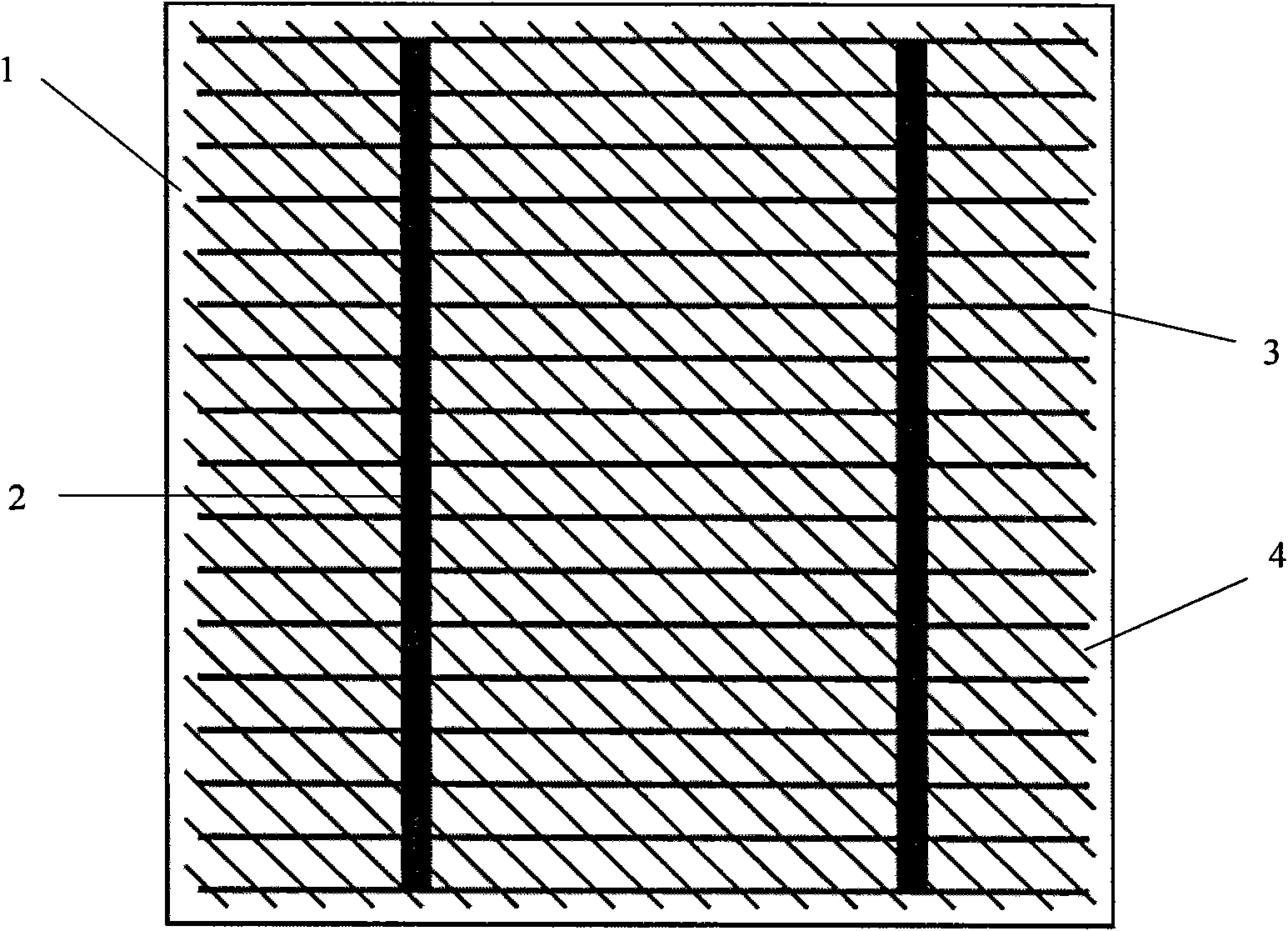
[0043] 3. Press figure 2 As shown in the figure, the phosphor paste is printed on the diffusion surface of the silicon wafer, and the figure forms a parallel line array with a line spacing of 0.8mm. The angle between the array and the straight edge of the wafer is 45°. Then put the silicon wafer into the chain diffusion furnace for rapid diffusion, so that the printed phosphorous paste area forms a highly doped area;
[0044] 4. Etch the edge of the silicon wafer to remove the peripheral PN junction;
[0045] 5. Deposit silicon nitride anti-reflection film on the diffusion surface;
[0...
PUM
| Property | Measurement | Unit |
|---|---|---|
| Line spacing | aaaaa | aaaaa |
| Sheet resistance | aaaaa | aaaaa |
| Sheet resistance | aaaaa | aaaaa |
Abstract
Description
Claims
Application Information