Method for preparing SiO2-containing metal oxide composite film

A composite film and oxide technology, which is applied in anodic oxidation, final product manufacturing, sustainable manufacturing/processing, etc., can solve the problems of battery efficiency decline and compound rate increase, and achieve the effect of convenient operation and simple and feasible process

Active Publication Date: 2012-02-29
INST OF ELECTRICAL ENG CHINESE ACAD OF SCI
View PDF0 Cites 0 Cited by
  • Summary
  • Abstract
  • Description
  • Claims
  • Application Information

AI Technical Summary

Problems solved by technology

[0003] The purpose of the present invention is to overcome the problem that the recombination rate of the back of the battery in the prior art increases and the battery efficiency is significantly lowered, and proposes a method for preparing SiO-containing 2 Method of Metal Oxide Composite Thin Films

Method used


Image

  • Method for preparing SiO2-containing metal oxide composite film
  • Method for preparing SiO2-containing metal oxide composite film
  • Method for preparing SiO2-containing metal oxide composite film

Examples


Embodiment 1

[0029] 1. Prepare N-type silicon wafers, go through the texturing process, rinse with ultrapure water, and blow dry;

[0030] 2. Silk-print Al slurry on the silicon wafer prepared in step 1, and then sinter it in a sintering furnace with a sintering peak temperature of 820°C and a time of 8s;

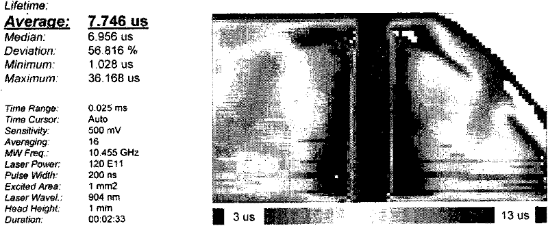
[0031] 3. Cut the silicon wafer prepared in step 2 into several small pieces, put them in a hydrochloric acid solution with a mass concentration of 37% and boil for 5 minutes to remove the Al layer and Al-Si alloy layer of the silicon wafer; then take out the silicon wafer and use Clean with ultrapure water and blow dry to obtain Al-doped P+ layer (effectively doped layer). Use Semilab WT2000 Minority Child Life Tester to test Minority Child Lifetime, the test results are as follows Figure 1a Shown

[0032] 4. The silicon wafer prepared in step 3 is etched in a potassium hydroxide solution with a mass concentration of 12% and a temperature of 55°C for 3 minutes to clean the surface traces of ...

Embodiment 2

[0039] 1. Prepare P-type silicon wafer, clean and blow dry according to standard RCA cleaning steps;

[0040] 2. Silk-print Al paste on the silicon wafer prepared in step 1, and then sinter it in a sintering furnace. The sintering peak temperature is 1050°C and the time is 2s;

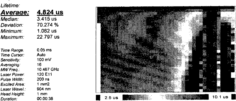
[0041] 3. Cut the silicon wafer prepared in step 2 into several small pieces, put them in a 10% phosphoric acid solution and react for 10 minutes at room temperature to remove the Al layer and Al-Si alloy layer of the silicon wafer; then take out the silicon wafer and use ultra-pure Wash with water and blow dry to obtain Al-doped P+ layer (effective doping layer). The semilab WT2000 minority carrier life tester is used to test the silicon wafer minority carrier lifetime, and the test results are as follows Figure 2a Shown

[0042] 4. Prepare 2 liters of nitric acid solution to be used as a conductive solution for anodizing process;

[0043] 5. Place the silicon wafer prepared in step 4 on the anode end of th...

Embodiment 3

[0047] 1. Prepare N-type silicon wafers, go through the texturing process, rinse with ultrapure water, and blow dry;

[0048] 2. Silk-print Al paste on the silicon wafer prepared in step 1, and then sinter the silicon wafer through a sintering furnace with a sintering peak temperature of 850°C and a time of 4s;

[0049] 3. Cut the silicon wafer prepared in step 2 into several small pieces, put them in a 10% hydrochloric acid solution and boil for 30 minutes to remove the Al layer and Al-Si alloy layer of the silicon wafer; then take out the silicon wafer and use super Clean with pure water and blow dry to obtain Al-doped P+ layer (effective doping layer);

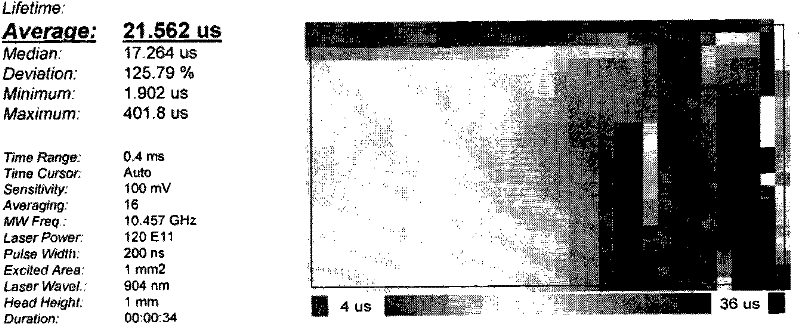
[0050] 4. Etch in a potassium hydroxide solution with a mass concentration of 15% and a temperature of 55°C for 20 seconds to clean the surface traces of the silicon wafer to obtain an Al-doped P+ inner layer (effectively doped layer inner layer). Use semilab WT2000 minority carrier lifetime tester to test the minority carrier li...


PUM


Abstract

The invention relates to a method for preparing a SiO2-containing metal oxide composite film, comprising the steps of: firstly, carrying out silk-screen to form a layer of metal slurry on the surface of a silicon wafer (1), sintering, and then removing a metal electrode layer and a metal-silicon alloy layer (3) on the surface of the silicon wafer (1) in a strongly acidic solution; then cleaning traces on the surface of the silicon wafer to obtain an effective doping layer (2) of the metal; or etching the silicon wafer (1) in an alkaline etching solution for 10s-12min to obtain an effective doping layer inlayer (2) of the metal; then preparing a SiO2-containing metal oxide composite film (4) by adopting an anodic oxidation method; and annealing to obtain the film as required.

Description

Technical field [0001] The invention relates to a method for preparing a silicon-based dielectric film, in particular to the preparation of 2 The method of metal oxide composite film. Background technique [0002] Metal oxide film such as Al 2 O 3 , HfO 2 , SiO 2 As a passivation film, the film has good passivation characteristics and excellent electrical properties. For the preparation of high-efficiency solar cells, usually due to factors such as the fracture of Si-Si bonds on the surface of the silicon wafer and impurities on the surface and in the body, a large number of dangling bonds and defect states will be formed on the surface of the silicon wafer. SiO is used 2 Passivation can form strong Si-O bonds, which can reduce the density and defect states of dangling bonds, thereby reducing the minority carrier recombination on the silicon surface. 2 O 3 Due to its special structure, it will exhibit negative charge characteristics, which has greater advantages for passivating th...

Claims


Application Information

Patent Timeline
Patent Type & Authority Patents(China)
IPC IPC(8): H01L31/18C25D11/32
CPCY02P70/50
Inventor 张俊王文静周春兰
Owner INST OF ELECTRICAL ENG CHINESE ACAD OF SCI
Why Eureka
Try Eureka