
Method for preparing black silicon based on liquid-phase chemical reaction

A liquid-phase chemical reaction, black silicon technology, applied in the fields of polysilicon and amorphous silicon surface texture, black silicon preparation, and monocrystalline silicon, can solve problems such as difficulty in obtaining large-scale promotion, high equipment investment, and limited application.

Inactive Publication Date: 2011-05-11
YUNNAN NORMAL UNIV
View PDF4 Cites 23 Cited by
  • Summary
  • Abstract
  • Description
  • Claims
  • Application Information

AI Technical Summary

Problems solved by technology

So far, the preparation technology of black silicon is mostly based on laser irradiation in a specific gas environment pioneered by Professor E. Mazur. Although this method is the most successful method at present, its high equipment investment is disappointing. , it is difficult to obtain large-scale promotion, which greatly limits the application of this method

Method used


Image

  • Method for preparing black silicon based on liquid-phase chemical reaction
  • Method for preparing black silicon based on liquid-phase chemical reaction

Examples


Embodiment 1

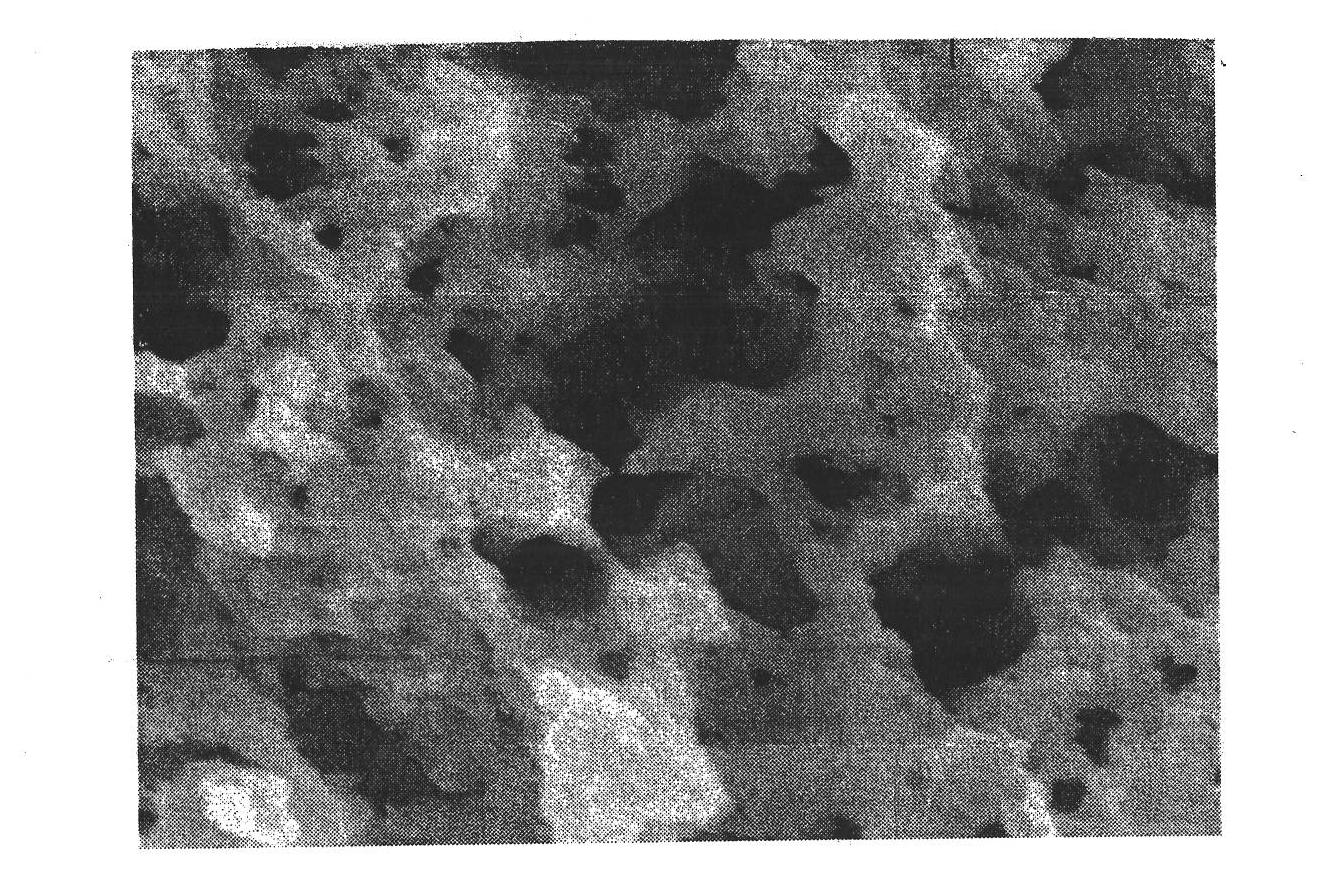
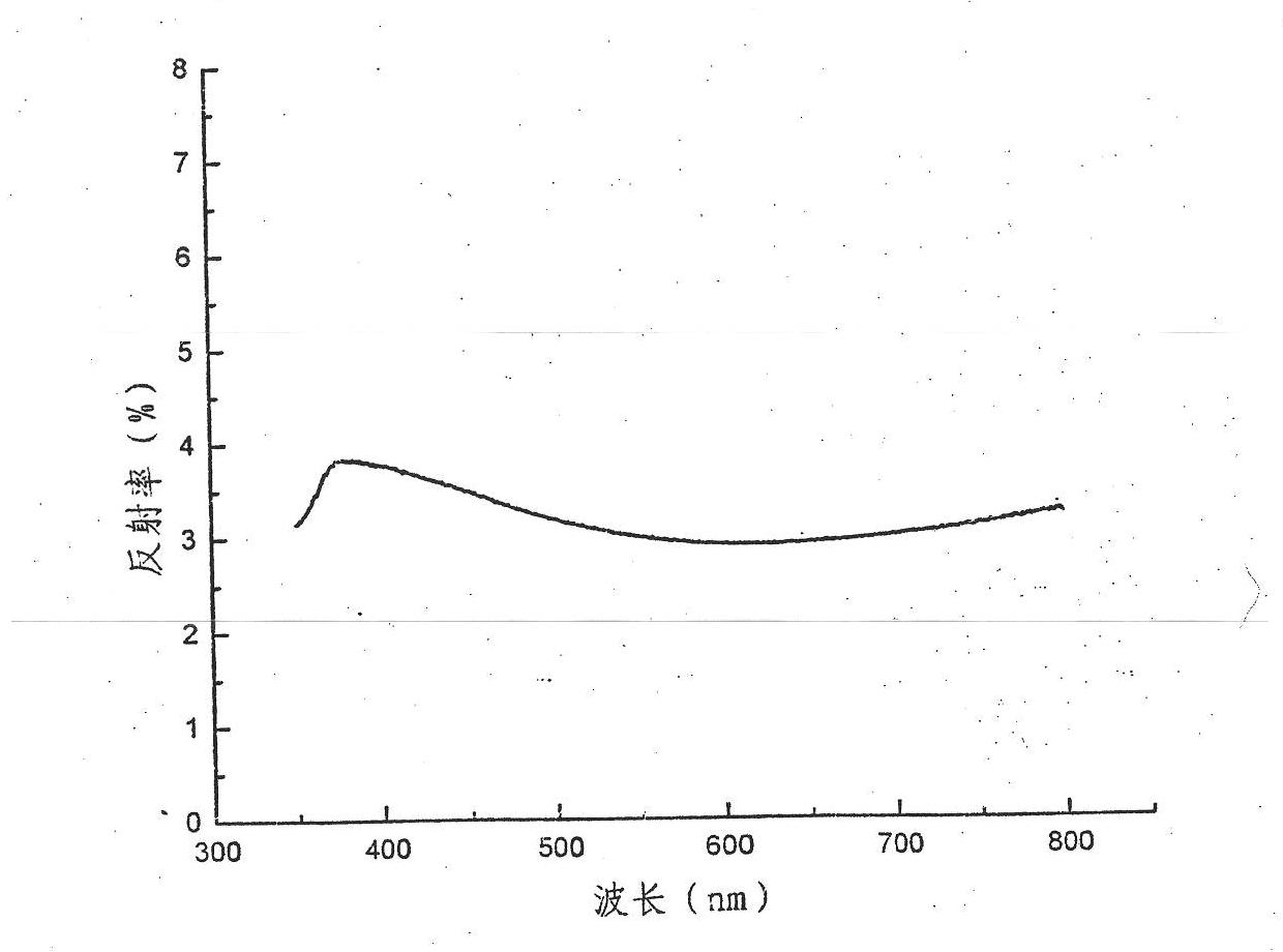
[0015] Embodiment 1: be 1: 4 configuration 100 milliliters mixed solutions by the weight ratio of hydrofluoric acid and hydrogen peroxide, wherein the weight percent concentration of hydrofluoric acid is 8%, and the weight percent concentration of hydrogen peroxide is 24%. Put the unpolished single crystal silicon chip into the solution heated to 15°C, then add 0.2 mmol of chloroauric acid, take out the silicon chip after 4.5 minutes, rinse it, and let it dry naturally. The prepared black silicon material absorbs more than 95% of the light in the wavelength range of 300-800nm. The SEM top view of black silicon material is as follows figure 1 as shown, figure 1 A structure of a large number of silicon micro-holes is formed on the surface of the black silicon material. figure 2 It shows that the light absorption of the black silicon material in the wavelength range of 300-800nm ​​is as high as 95%.

Embodiment 2

[0016] Embodiment 2: be 1: 3 configuration 100 milliliters mixed solutions by the weight ratio of hydrofluoric acid and hydrogen peroxide, wherein the weight percent concentration of hydrofluoric acid is 5%, and the weight percent concentration of hydrogen peroxide is 10%. Heat the solution to 50°C, put the monocrystalline silicon wafer into the mixed solution heated to 25°C, then add 1 mmol of silver nitrate, take out the silicon wafer after 60 minutes, rinse it, and dry it naturally to prepare the black silicon material .

Embodiment 3

[0017] Embodiment 3: be 1: 6 configuration two parts of identical 100 milliliters mixed solutions by the weight ratio of hydrofluoric acid and hydrogen peroxide, wherein the weight percent concentration of hydrofluoric acid is 20%, the weight percent concentration of hydrogen peroxide 0.5%. Put the monocrystalline silicon chip into the first solution heated to 25°C, then add 1 mmol of silver nitrate, take out the silicon chip after 1 minute; heat the other solution to 50°C, put the silicon chip into Immediately, 2 mmol of ferric nitrate was added to the solution, and after 50 minutes, the silicon chip was taken out, rinsed, and dried naturally to prepare a black silicon material.


PUM


Abstract

The invention relates to a method for preparing black silicon based on liquid-phase chemical reaction, comprising the following steps of: placing a silicon slice in a corrosive solution; then adding a metal compound to the corrosive solution; and carrying out texturing treatment on the surface of the silicon slice through ion etching reaction under catalysis to form a black silicon material with a microstructural surface. By carrying out surface texturing of a nano scale on the silicon surface, the band absorption and reflectivity of the product can be effectively controlled so that the conversion efficiency of a silicon-based solar battery can be improved. The method can be applied to preparing large-area black silicon material, and the surface of the prepared black silicon material contains microstructures, such as a silicon microcolumn, a silicon particle, silicon microholes and the like. The light absorption of the black silicon material in the wavelength range of 300-2000nm can be up to over 90%, and the light absorption in the wavelength range of 300-800nm can be up to over 95%.

Description

technical field [0001] The invention relates to a method for preparing black silicon based on liquid phase chemical reaction, in particular to a method for performing surface texture of single crystal silicon, polycrystalline silicon and amorphous silicon by reactive ion etching in liquid phase. Belongs to the technical field of semiconductor optoelectronic materials preparation, Background technique [0002] Among the current commercial solar cell products, silicon-based solar cells have the largest market share. However, one of the bottleneck technologies restricting silicon-based solar cells is that it is difficult to further improve the solar energy conversion efficiency. Therefore, the surface modification of silicon-based materials and Micro-nano texturing has become a hot spot in the research of silicon-based solar cells recently. Among them, forming black silicon on the surface of silicon to effectively reduce the reflection of solar cells to sunlight is a very effe...

Claims


Application Information

Patent Timeline
Patent Type & Authority Applications(China)
IPC IPC(8): C23F1/24C23F1/02C30B33/10
Inventor 杨培志李学铭廖承菌杨雯田晶郝瑞亭
Owner YUNNAN NORMAL UNIV
Learn More