GaN-based semiconductor laser and manufacturing method thereof

A gallium nitride-based, manufacturing method technology, applied in semiconductor lasers, lasers, laser parts and other directions, can solve problems such as increased defect density, high resistivity, and low hole concentration

Inactive Publication Date: 2011-05-18
BEIJING UNIV OF CHEM TECH
View PDF5 Cites 13 Cited by
  • Summary
  • Abstract
  • Description
  • Claims
  • Application Information

AI Technical Summary

Problems solved by technology

Due to the large ionization energy of acceptor impurities in P-type GaN and P-type AlGaN, for example, the ionization energy of magnesium impurities in GaN is between 0.16eV and 0.20eV, such a large ionization energy makes the ionization rate of magnesium impurities less than 1%, while Increasing the doping concentration of magnesium will cause the decrease of crystal quality and the increase of defect density, so that the ionized magnesium will be compensated by the increased donor, but the hol...

Method used


Image

  • GaN-based semiconductor laser and manufacturing method thereof
  • GaN-based semiconductor laser and manufacturing method thereof
  • GaN-based semiconductor laser and manufacturing method thereof

Examples


Embodiment 1

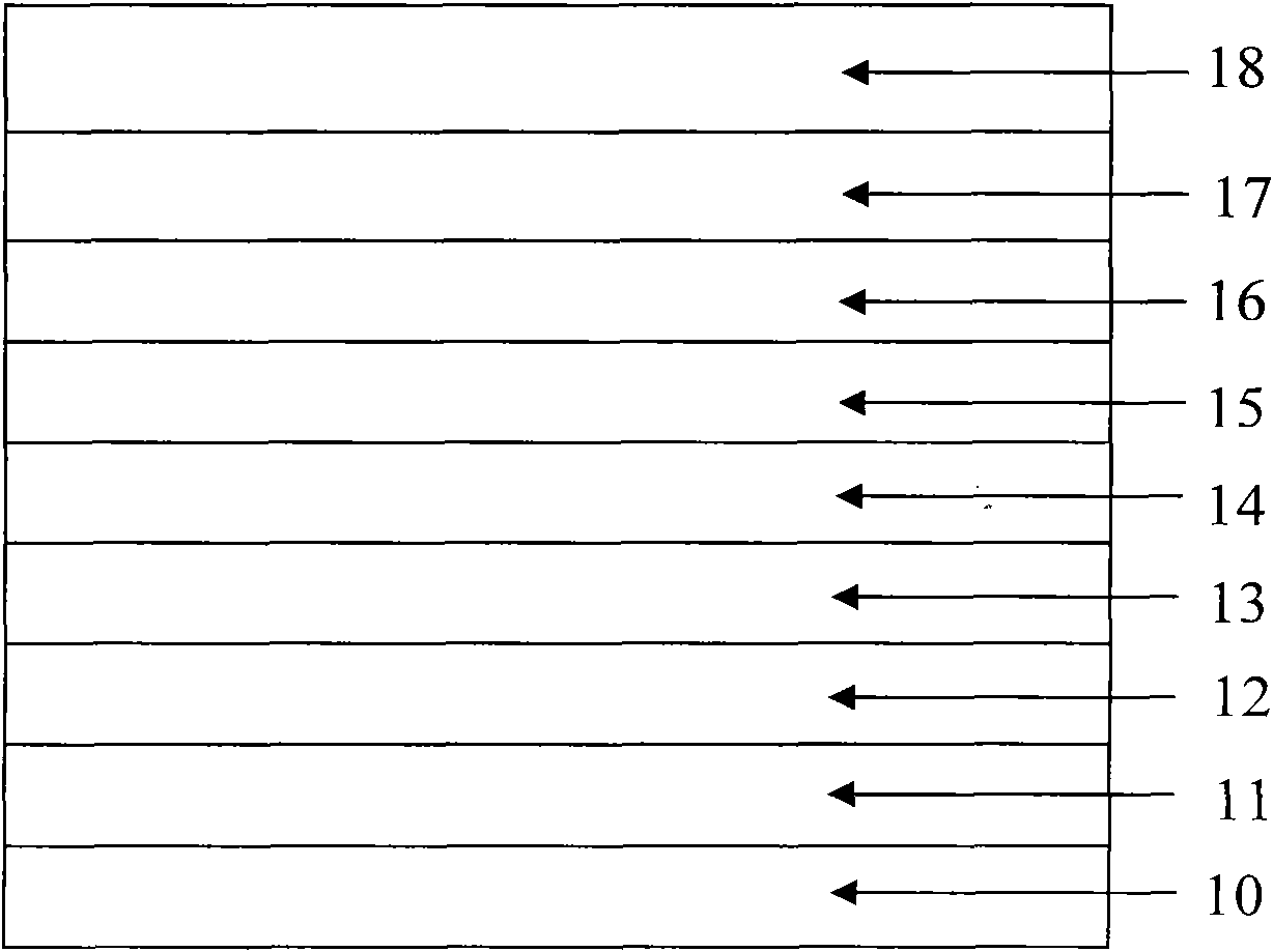
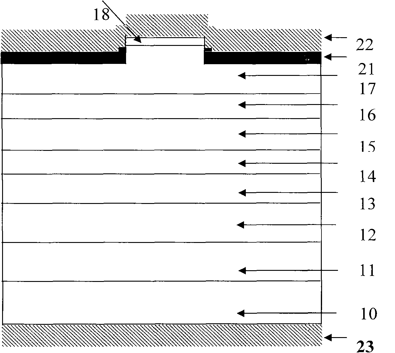
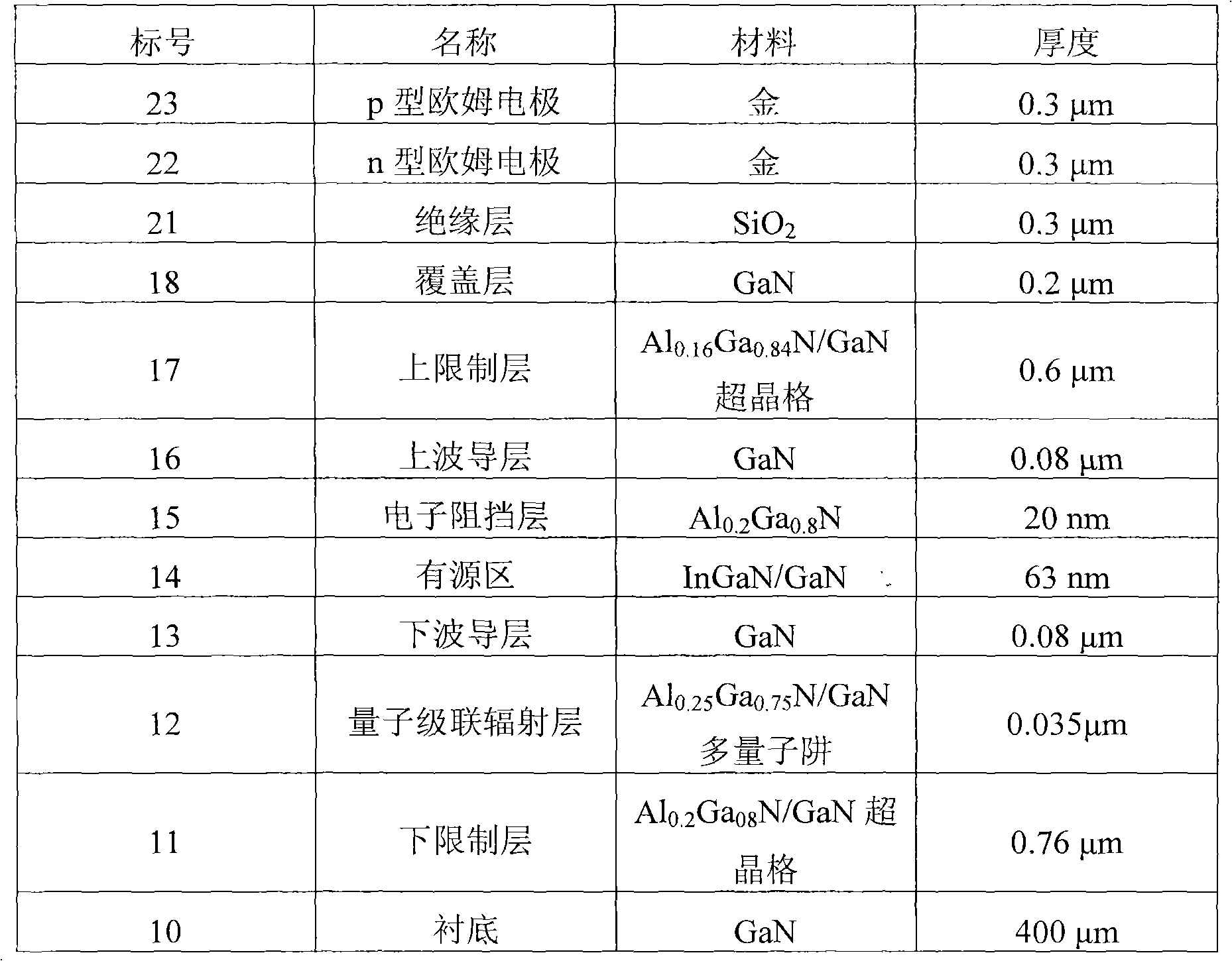
[0032] In order to further illustrate the effect of the device structure, we take a GaN-based semiconductor laser with an operating wavelength of 405nm as an example to illustrate the preparation process of the device structure. The material and thickness of each layer are shown in Table 1. The details are as follows: the device structure is grown on the n-type (0001)-plane gallium nitride substrate 10 by MOCVD method. The structure includes n-type Al 0.2 Ga 0.8 N / GaN superlattice lower confinement layer 12 (thickness is 0.76 μm, GaN well width is 2.0nm, Al 0.2 Ga 0.8 N barrier width is 2.0nm, doping concentration is 3×10 18 cm -3 ), n-type Al 0.30 Ga0.70 N / GaN multi-quantum well quantum cascade radiation layer 12 [this layer has three periods in total, and each period is Al from bottom to top 0.30 Ga 0.70 N(1.9nm) / GaN(2.6nm) / Al 0.30 Ga 0.70 N(1.9nm) / GaN(1.6nm) / Al 0.30 Ga 0.70 N(1.4nm) / GaN(1.6nm), the doping concentration is 3×10 17 cm -3 ], n-type GaN lower wave...

Embodiment 2

[0035] In order to further illustrate the effect of this device structure, as a comparison, we take a GaN-based laser with an operating wavelength of 405nm that does not include an AlGaN / GaN multi-quantum well quantum cascade radiation layer as an example. Except that the GaN-based laser device structure does not include the AlGaN / GaN multi-quantum well quantum cascade radiation layer and the thickness of the lower confinement layer is increased to 0.8 μm, the parameters, growth conditions, device dimensions and manufacturing process of other layers are completely the same as those in Example 1. same. After testing, the threshold current of the device is 110mA, and the corresponding working voltage is 7.5V. The device has a working life of only 20 hours at 1.1 times the threshold current.

Embodiment 3

[0037] In order to illustrate the application value of the present invention, we take a GaN-based semiconductor laser with an operating wavelength of 450 nm as an example to illustrate the characteristics of the device structure. Compared with Example 1, the material and thickness of each layer are changed to In except for the active area 0.3 Ga 0.7 N / In 0.02 Ga 0.98 N multiple quantum wells (multiple quantum wells are 3 periods, In 0.3 Ga 0.7 N well width is 3nm, In 0.02 Ga 0.98 N barrier width is 5nm, Si impurity concentration is 3×10 16 cm -3 ), the quantum cascade radiation layer is n-type Al 0.25 Ga 0.75 N / GaN multiple quantum wells, a total of three periods, each period is Al from bottom to top 0.25 Ga 0.75 N(2.1nm) / GaN(2.8nm) / Al 0.25 Ga 0.75 N(2.1nm) / GaN(1.8nm) / Al 0.25 Ga 0.75 N(1.6nm) / GaN(1.8nm), the doping concentration is 3×10 17 cm -3 In addition, the parameters, growth conditions, device dimensions and fabrication process of other layers are exactl...


PUM


Abstract

The invention relates to a GaN-based semiconductor laser and a manufacturing method thereof, belonging to the field of semiconductor lasers. The device has the structure that a quantum cascade radiation layer is introduced between an n-type optical confinement layer and an n-type waveguide layer of the laser. By applying infrared radiation generated by the quantum cascade radiation layer when the laser works, the ionization of magnesium acceptor impurities in a p-type GaN waveguide layer, a p-type AlGaN optical confinement layer and a p-type GaN covering layer is realized, the carrier concentration of each p-type layer is increased, and the working voltage of the laser is reduced. The average Al component of the quantum cascade radiation layer is close to that of an n-type AlGaN optical confinement layer, thus the optical confinement factor of the laser has no obvious change. Although the voltage drop of the n-type layers can be increased when the laser works, the laser can still work at a lower voltage because the voltage drop of the p-type layers is greatly reduced. By applying the structure of the laser, the series resistance of the laser can be reduced to further reduce the working voltage of the laser and prolong the service life of the laser.

Description

technical field [0001] The invention belongs to the field of semiconductor devices, in particular to a gallium nitride-based semiconductor laser and a manufacturing method thereof. Background technique [0002] As a third-generation semiconductor, gallium nitride (GaN) and its series of materials (including aluminum nitride, aluminum gallium nitride, indium gallium nitride, and indium nitride) are characterized by their large band gap and wide spectral range (covering from ultraviolet to Infrared full band), high temperature resistance and corrosion resistance, it has great application value in the field of optoelectronic devices and microelectronic devices. GaN-based lasers are very important GaN-based optoelectronic devices. Because the light waves emitted by them are in the blue-violet light band, GaN-based lasers are used in high-density optical information storage, projection display, laser printing, underwater communication, activation of biochemical reagents and It h...

Claims


Application Information

Patent Timeline
IPC IPC(8): H01S5/343
Inventor 李德尧许海军朱建军张书明苏雷廛宇飞
Owner BEIJING UNIV OF CHEM TECH
Why Eureka
Try Eureka