Method for manufacturing photoelectric detection unit or focal plane device by using molecular beam epitaxy method

A technology of molecular beam epitaxy and photoelectric detection, which is applied in the direction of electrical components, semiconductor devices, chemical instruments and methods, etc., can solve the problems of complex process, affecting device performance, and difficulty in uniform material diffusion, and achieve high doping efficiency and atomic radius small effect

Inactive Publication Date: 2011-07-20
SHANGHAI INST OF MICROSYSTEM & INFORMATION TECH CHINESE ACAD OF SCI
View PDF1 Cites 3 Cited by
  • Summary
  • Abstract
  • Description
  • Claims
  • Application Information

AI Technical Summary

Problems solved by technology

Epitaxial in-situ doping to form a junction Since the pn junction is naturally and continuously completed during the material growth process, the general junction quality is better and more convenient, and it is also easy to form a sudden junction. The influence of the side wall will bring certain difficulties to passivation, and it will affect the performance of the device when the passivation effect is not good. Due to its non-planarity, the mesa structure will also bring restrictions to some applications that require device planarization. Sometimes it is necessary to use Special planarization measures; diffusion or ion implantation after epitaxial doping into a junction, the sidewall of the pn junction is generally surrounded by a cap layer material with a wide bandgap, the general passivation effect is better, which is conducive to improving device performance, and it is easy to make a plane device, but it also brings more complicated problems in the subsequent process
For the diffusion process, its pn junction pattern is not easy to be accurately defined, and for the III-V family diffusion process, there is also the problem that the diffusion of larger-sized materials is not easy to be uniform, which has a particularly significant impact on larger-scale focal plane array devices; for Ion implantation, high-temperature annealing after implantation brings difficulties to the subsequent process, and the implantation damage is difficult to completely eliminate, which is also very unfavorable for photodetection devices with high requirements

Method used


Image

  • Method for manufacturing photoelectric detection unit or focal plane device by using molecular beam epitaxy method
  • Method for manufacturing photoelectric detection unit or focal plane device by using molecular beam epitaxy method

Examples


Embodiment approach

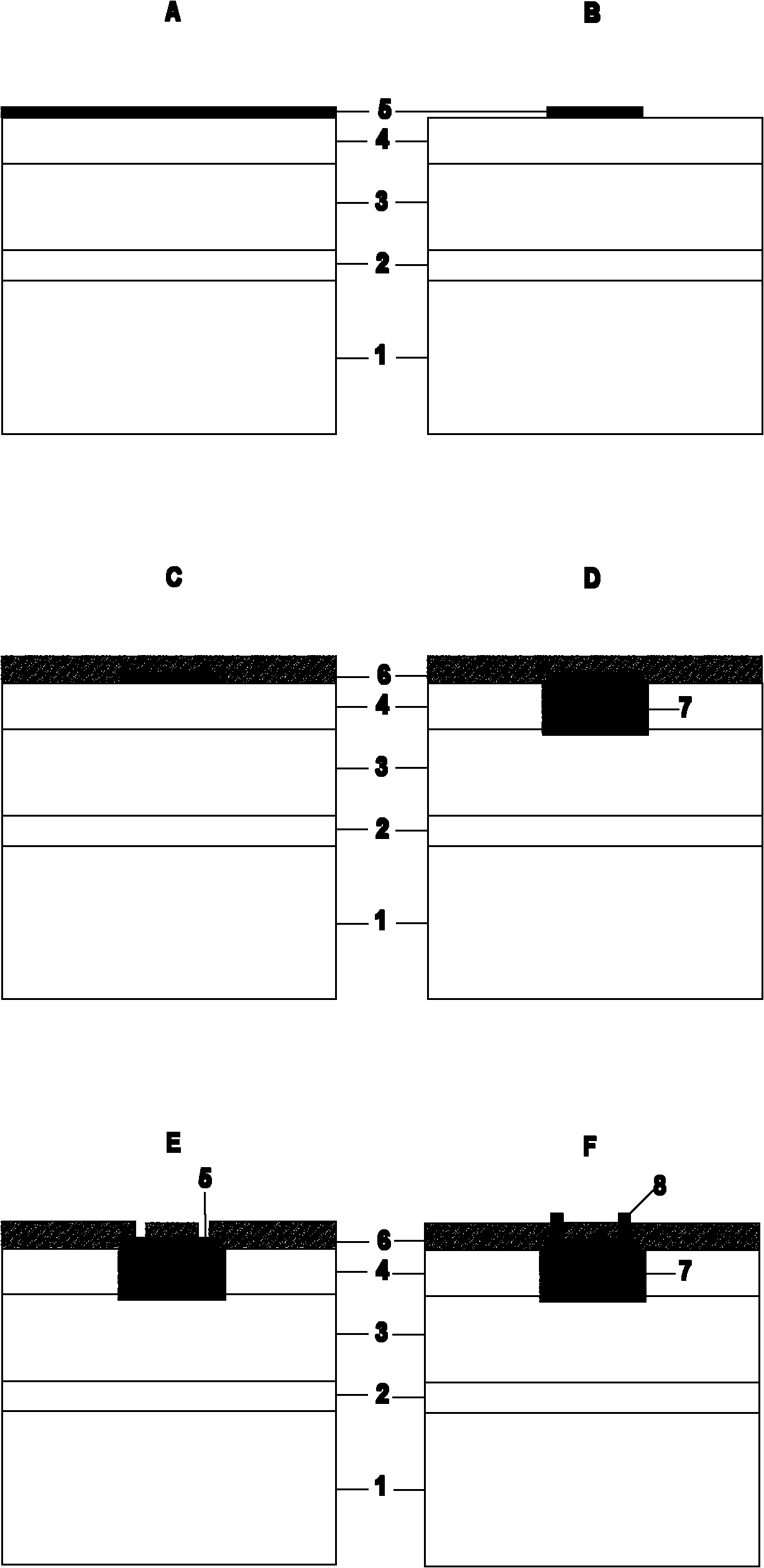
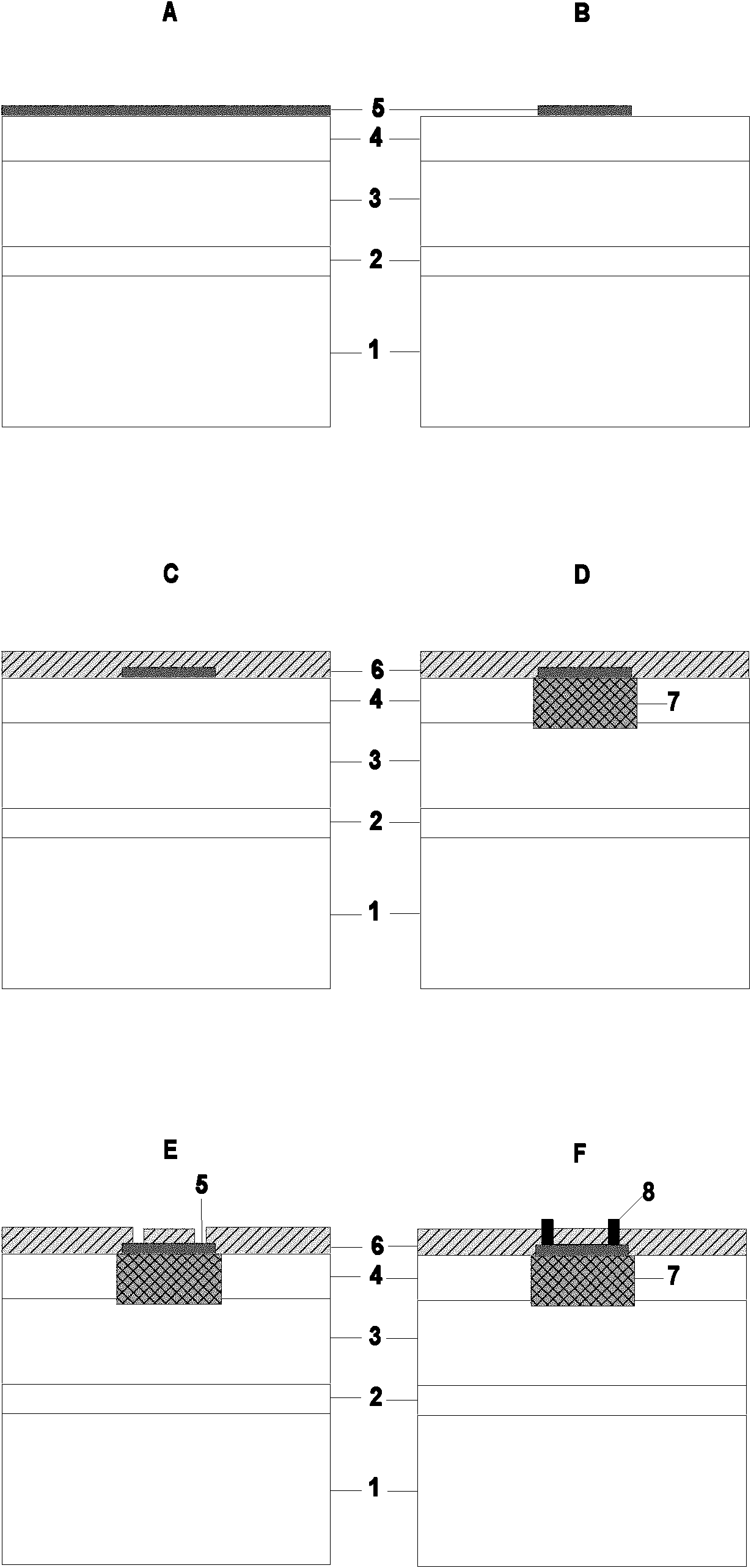
[0023] (1) At first, the molecular beam epitaxy growth technology is used to grow on the InP substrate (1 in the accompanying drawing), including the buffer layer (2 in the accompanying drawing), the InGaAs light absorption layer (3 in the accompanying drawing) and the wide bandgap cap layer (1 in the accompanying drawing). 4) in the figure is suitable for the epitaxial structure of the photodetector device of the planar diffusion process. The InP substrate can be semi-insulating or N-type highly doped conductivity type according to the specific requirements of the device (such as front or back light, packaging and application requirements, etc.); the buffer layer can use wide bandgap such as InP or InAlAs (relative to the absorption layer and The thickness of the material is 500 nanometers, and the doping and its concentration can also be determined according to the final requirements of the device; the InGaAs light absorption layer is unintentionally doped or low-doped n-type...

Embodiment 2

[0031] The embodiment of the present invention is specifically described below by taking the fabrication of a GaAs photodetector device on a GaAs substrate as an example:

[0032] (1) At first, the molecular beam epitaxy growth technique is used to grow on the GaAs substrate (1 in the accompanying drawing), including the buffer layer (2 in the accompanying drawing), the GaAs light absorbing layer (3 in the accompanying drawing) and the wide bandgap AlGaAs cap layer (2 in the accompanying drawing). The epitaxial structure of the photodetection device suitable for planar diffusion process in 4) of the accompanying drawings. The GaAs substrate can use semi-insulating or N-type highly doped conductivity type according to the specific requirements of the device (such as front or back light, packaging and application requirements, etc.); the buffer layer can be GaAs material, the thickness is 500 nanometers, the doping and its concentration It can also be determined according to the...


PUM

PropertyMeasurementUnit
thicknessaaaaaaaaaa
thicknessaaaaaaaaaa
thicknessaaaaaaaaaa

Abstract

The invention relates to a method for manufacturing a photoelectric detection unit or a focal plane device by using a molecular beam epitaxy method, comprising the steps of: growing a buffer layer, a light absorption layer and an epitaxial structure of a wide bandgap cap layer on a conductive substrate by applying a molecular beam epitaxial growth technology, and then continuously growing a high-Be-doped or delta-doped heterogeneous narrow bandgap lamella to serve as a diffusion source layer; and (2) etching the diffusion source layer by using a conventional graph processing technology to form a locally doped source graph, forming a pn (positive negative) junction under the protection of a passivated dielectric film by applying a diffusion technology at the diffusion temperature of 450-600 DEG C, and then, manufacturing an electrode to form the photoelectric detection unit or the focal plane device. The method provided by the invention has the advantages of universality and simplicity, a doping junction-forming process is combined with the advantages of junction-forming convenience of a table-board type in-situ doping junction-forming process and good passivation effect of a planer type diffusion junction-forming process in the manufacturing of the photoelectric detection unit, the device process is simplified and the device property is improved.

Description

technical field [0001] The invention belongs to the field of preparation of a photoelectric detection unit or a focal plane device, in particular to a method for manufacturing a beryllium diffusion source by a molecular beam epitaxy method to form a plane / quasi-planar photodetection unit or a focal plane device. Background technique [0002] Semiconductor photodetectors are generally quantum detectors. Its invention has a history of more than 100 years. It can use various semiconductor materials and has important applications in many fields. The structure of semiconductor photodetectors has developed from simple bulk materials to complex microstructure materials such as heterojunctions, quantum wells, and superlattices. Visible, near-infrared, mid-infrared and even far-infrared bands, material systems also include VI, III-V, II-VI, IV-VI and organic compounds, etc., as well as photoconductive, photovoltaic and other types, and so on. The common ones are photovoltaic photode...

Claims


Application Information

Patent Timeline
Patent Type & Authority Applications(China)
IPC IPC(8): H01L31/18C30B29/40C30B25/02
CPCY02P70/50
Inventor 张永刚顾溢
Owner SHANGHAI INST OF MICROSYSTEM & INFORMATION TECH CHINESE ACAD OF SCI
Why Eureka
Try Eureka