Novel transparent conducting oxide thin film with multi-layer film structure and manufacturing method thereof
An oxide thin film, transparent and conductive technology, which is applied in chemical instruments and methods, coatings, circuits, etc., can solve the problems of slow film growth and no suede structure on the film surface, so as to reduce material costs and achieve good photoelectric performance , the effect of low price
- Summary
- Abstract
- Description
- Claims
- Application Information
AI Technical Summary
Problems solved by technology
Method used
Image
Examples
Embodiment 1
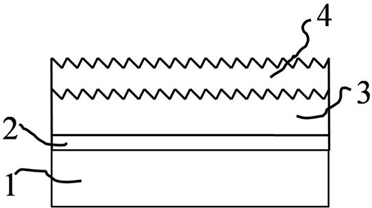
[0033] The structure of the transparent conductive oxide film with multilayer film structure is: the substrate is ultra-clear glass, the thickness is 3.2mm; the transition layer is SiO 2 , with a thickness of 70nm; the thickness of the ITO film is 500nm; the thickness of the Al-doped ZnO film is 500nm. All layers were deposited at 300°C using Ar and O 2 mixed gas, where O2 The content is 1%. The prepared samples were cleaned with deionized water at room temperature. After drying, the samples were put into 0.5wt% dilute hydrochloric acid for corrosion reaction. The reaction time was 10S, and the solution temperature was constant at 25 degrees Celsius. Finally, they were rinsed with deionized water at room temperature and dried.
Embodiment 2
[0035] The structure of the transparent conductive oxide film with multi-layer film structure is: the substrate is ultra-clear glass, the thickness is 3.2mm; the transition layer is SiN x , x is 0.1, and the thickness is 100nm; the thickness of the ITO film is 10nm; the thickness of the Al-doped ZnO film is 800nm. deposited SiN x The temperature is 500°C, the temperature for depositing the ITO layer is 300°C, and the temperature for depositing the Al-doped ZnO thin film is 200°C to 350°C. Figure 6 The resistivity as a function of AZO layer deposition temperature is shown.
Embodiment 3
[0037] The structure of the transparent conductive oxide film with multi-layer film structure is: the substrate is ultra-clear glass, the thickness is 3.2mm; the transition layer is SiN x , x is 1.5, and the thickness is 10nm; the thickness of the ITO film is 10nm; the thickness of the Ga-doped ZnO film is 1000nm. deposited SiN x The temperature is room temperature, and the deposition temperature of the ITO layer is room temperature. The ZnO-based TCO film layer is deposited with a Ga-doped ZnO film, and the target used is a 0.57wt% Ga-doped ZnO target. Wash the sample with deionized water, put the sample into 0.1mol / L oxalic acid for corrosion reaction after drying, the reaction time is 1 second to 400 seconds, the temperature of the acid solution is 25 degrees Celsius, because the oxalate generated by the reaction is relatively insoluble Therefore, during the cleaning process with deionized water, the temperature is controlled at 60 degrees Celsius, and finally dried. Fig...
PUM
| Property | Measurement | Unit |
|---|---|---|
| thickness | aaaaa | aaaaa |
| thickness | aaaaa | aaaaa |
| thickness | aaaaa | aaaaa |
Abstract
Description
Claims
Application Information


