Preparation method for stannum, indium and stibium series lead-free solder tinning copper strip used for solar battery

A solar cell, tin, indium and antimony system technology, applied in circuits, electrical components, final product manufacturing, etc., can solve the problems of high waste liquid treatment cost, serious environmental pollution, and few applications, and achieve extended fatigue life and interface bonding. Good, lower melting enthalpy effect

Inactive Publication Date: 2011-09-07
TIANJIN UNIV
View PDF6 Cites 11 Cited by
  • Summary
  • Abstract
  • Description
  • Claims
  • Application Information

AI Technical Summary

Problems solved by technology

The electroplating process is not widely used due to its high energy consumpt

Method used


Image

  • Preparation method for stannum, indium and stibium series lead-free solder tinning copper strip used for solar battery
  • Preparation method for stannum, indium and stibium series lead-free solder tinning copper strip used for solar battery
  • Preparation method for stannum, indium and stibium series lead-free solder tinning copper strip used for solar battery

Examples


Embodiment 1

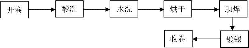
[0025] Pure tin, indium, and antimony are weighed in a mass ratio of 99:0.5:0.5, and the antimony and tin are heated and melted in a melting furnace at a ratio of 1:10 to form a tin-antimony master alloy. The remaining tin and indium are heated and melted to form a tin-antimony master alloy. Then heat and melt the two intermediate alloys, stir and water-cool at the same time to obtain Sn-0.5%In-0.7%Sb lead-free solder. Then it is dip-plated on the copper strip to form a tin-plated copper strip under the conditions of the traditional hot-dip plating production process, such as figure 1 Shown: pickling is to clean the copper strip in hydrochloric acid with a concentration of 10%, and water washing is to clean it in pure water, both of which are to remove the oxide layer and impurities on the surface of the copper strip. After drying, pass the copper strip through a container containing flux, and then through a tin melting furnace. The temperature of the tin melting furnace shou...

Embodiment 2

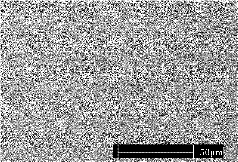
[0027] Sn, indium and antimony with a purity of 99.99% are weighed in a mass ratio of 96:1.5:2.5, antimony and tin are heated and melted in a smelting furnace at a ratio of 1:10 to form a tin-antimony master alloy, and then water-cooled and solidified. The remaining tin and indium are heated and melted in a smelting furnace to form a tin-antimony master alloy. Then heat and melt the two intermediate alloys in a melting furnace to obtain Sn-1.5%In-2.5%Sb lead-free solder. It is then dip-plated on copper strips to form tinned copper strips under conventional hot-dip plating production process conditions. Its microstructure is as image 3 As shown, the matrix in the alloy structure is β-Sn phase. Due to the high content of In and Sb, a large number of granular and rod-shaped intermetallic compounds InSb are distributed on the matrix. The particles are InSb phase, the alloy has a lower melting point (186°C), which is close to the traditional Sn-Pb solder for tin plating, and has...

Embodiment 3

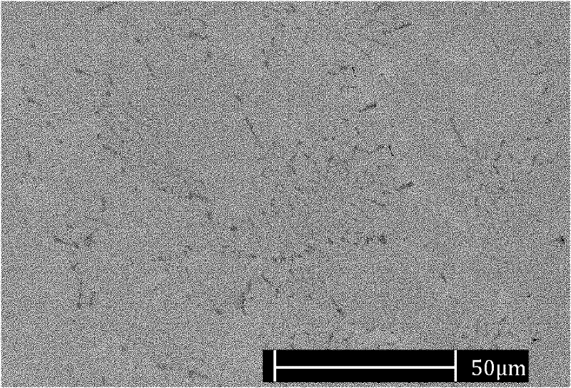
[0029] Pure tin, indium and antimony are weighed in a mass ratio of 83:9:8, antimony and tin are heated and melted in a melting furnace at a ratio of 1:10 to form a tin-antimony master alloy. The remaining tin and indium are heated and melted in a smelting furnace to form a tin-antimony master alloy, which is then cooled and solidified. Then heat and melt the two intermediate alloys in a melting furnace to obtain Sn-9%In-8%Sb lead-free solder. It is then dip-plated on copper strips to form tinned copper strips under conventional hot-dip plating production process conditions. Its microstructure is as Figure 4 As shown, the matrix in the alloy structure is β-Sn phase, and granular and rod-shaped intermetallic compounds InSb are distributed on the matrix. The particles are InSb phase, with a melting point of about 191°C, high hardness and tensile strength, and good ductility, which meets the basic requirements of solar cells for the current-carrying capacity of the busbar, and...


PUM

PropertyMeasurementUnit
Melting pointaaaaaaaaaa

Abstract

The invention relates to a preparation method for a stannum, indium and stibium series lead-free solder tinning copper strip used for a solar battery. The preparation method comprises the following steps: pure stannum, indium and stibium, as well as bismuth, copper and silver are weighted according to the mass ratio of (83-99):(0.5-9):(0.1-8):(0-4):(0-1):(0-1); firstly, stibium, copper and silver are melted along with stannum in a smelting furnace in the proportion of 1:10 and then stirred to enable the stibium, copper and silver to be completely melted in stannum, and a stannum, stibium, silver and copper intermediate alloy is formed; secondly, the residual stannum and the other components are melted to form corresponding intermediate alloys; then two intermediate alloys are melted and stirred to be evenly mixed; and finally, the traditional hot dip-soldering process is used, and lead-free solder is dip-soldered on a copper wire or a copper strip. The Sn-In-Sb series lead-free solder has very low silver content, the solder cost is greatly lowered, the copper strip has better ductility and tensile strength, and the connection interface has high reliability. The high-performance solder alloy is taken as the object of study and is enabled to meet the industrial application requirements, so that the development prospect is good.

Description

technical field [0001] The invention belongs to the field of basic materials in the electronic industry, in particular to a preparation method of lead-free solder and tinned copper wire or copper strip. Background technique [0002] When non-renewable energy sources such as electricity, coal, and oil are running out frequently, and energy issues have increasingly become a bottleneck restricting the development of the international society and economy, more and more countries have begun to implement the "Sunshine Plan" to develop solar energy resources and seek new impetus for economic development. It can be said that solar energy is an inexhaustible clean energy. At present, the main way to convert solar energy into electrical energy is solar cells. Solar cells can ensure a win-win situation for the economy and the environment, and there are fewer constraints than wind power generation. Humans may use solar cells to replace fossil energy on a larger scale in the foreseeable ...

Claims


Application Information

Patent Timeline
IPC IPC(8): C22C1/03C22C13/00C22C13/02H01L31/18
CPCY02P70/50
Inventor 刘永长董明杰高志明余黎明
Owner TIANJIN UNIV
Why Eureka
Try Eureka