Manufacturing method of tunable triangular metal nano particle array structure

A metal nanoparticle and array structure technology, applied in nanotechnology, microstructure technology, microstructure devices and other directions, can solve the problems of high processing cost and time-consuming, and achieve low cost, controllable optical properties, and obvious extinction spectrum peak. Effect

Inactive Publication Date: 2011-09-14
INST OF OPTICS & ELECTRONICS - CHINESE ACAD OF SCI
View PDF4 Cites 39 Cited by
  • Summary
  • Abstract
  • Description
  • Claims
  • Application Information

AI Technical Summary

Problems solved by technology

Although electron beam lithography and focused ion beam have the advantages of ...

Method used


Image

  • Manufacturing method of tunable triangular metal nano particle array structure
  • Manufacturing method of tunable triangular metal nano particle array structure
  • Manufacturing method of tunable triangular metal nano particle array structure

Examples


Embodiment 1

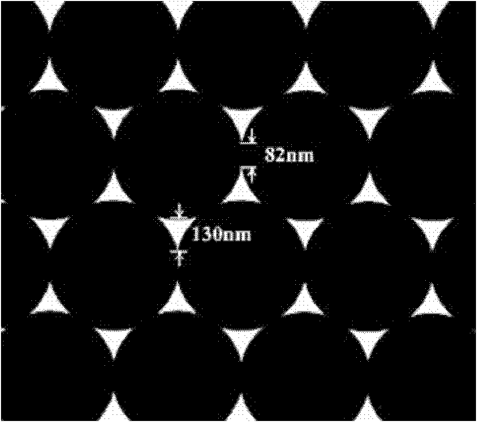
[0031] Example 1, using the present invention to realize the fabrication of a triangular silver nanoarray structure with a particle diameter of 130nm, a gap between adjacent particle tips of 82nm, and a thickness of 50nm.

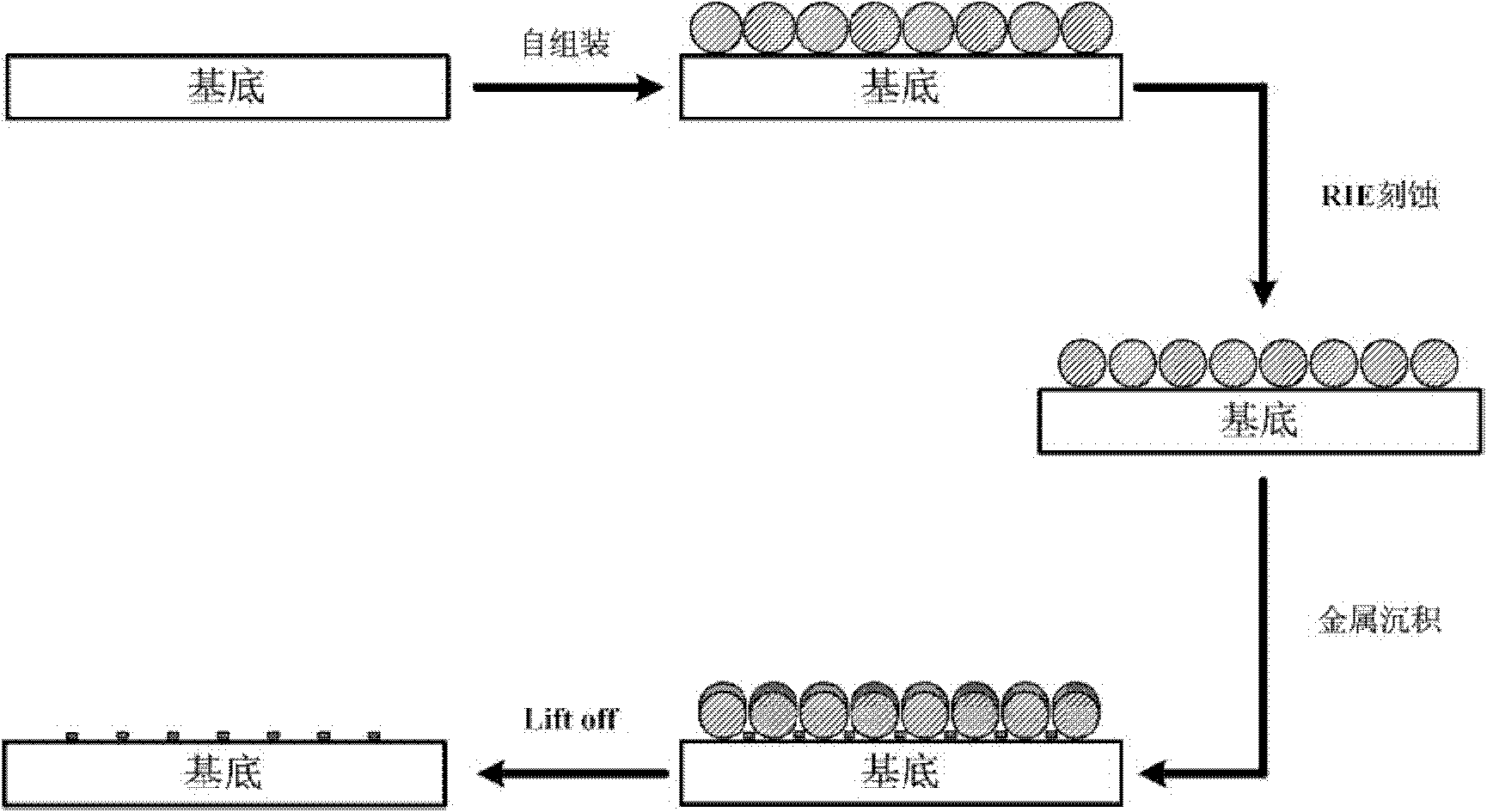
[0032] (1) Select K9 glass with a size of 10mm×20mm×10mm as the chip substrate, and clean and hydrophilize the substrate;

[0033] (2) 6 μL of an aqueous solution of monodisperse polystyrene nanospheres with a diameter of 430 nm and a concentration of 10% was dropped onto a glass substrate for self-assembly, and dried at room temperature to obtain a polystyrene nanosphere array arranged in a single layer;

[0034] (3) Etching the self-assembled polystyrene nanospheres with a reactive ion etching machine using oxygen, the power is 5W, the oxygen flow rate is 20SCCM, and the etching time is 2min respectively;

[0035] (4) Put the etched polystyrene nanospheres into the working chamber of the vacuum coating system, -4 Deposit a layer of silver film on its sur...

Embodiment 2

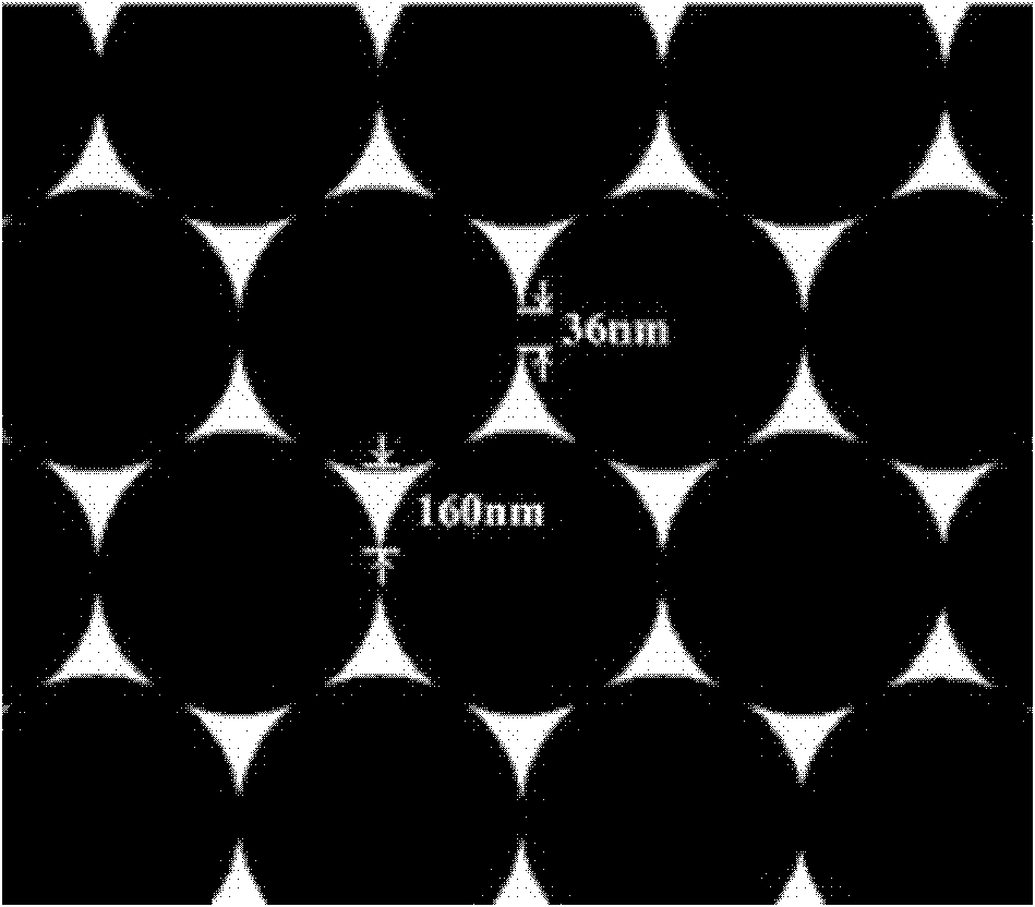
[0038] Example 2, using the present invention to realize the fabrication of a triangular silver nanoarray structure with a particle diameter of 160nm, a gap between adjacent particle tips of 36nm, and a thickness of 50nm.

[0039] (1) Select quartz with a size of 10mm×10mm×10mm as the chip substrate, and clean and hydrophilize the substrate;

[0040] (2) 6 μL of an aqueous solution of monodisperse polystyrene nanospheres with a diameter of 430 nm and a concentration of 10% was dropped onto a glass substrate for self-assembly, and dried at room temperature to obtain a polystyrene nanosphere array arranged in a single layer;

[0041] (3) Etching the self-assembled polystyrene nanospheres with a reactive ion etching machine using oxygen, the power is 5W, the oxygen flow rate is 20SCCM, and the etching time is 4min;

[0042] (4) Put the etched polystyrene nanospheres into the working chamber of the vacuum coating system, -4 Deposit a layer of silver film on its surface under the ...

Embodiment 3

[0045] Example 3, using the present invention to realize the fabrication of a triangular silver nanoarray structure with a particle diameter of 140nm, a gap between adjacent particle tips of 40nm, and a thickness of 40nm.

[0046] (1) Select quartz with a size of 10mm×10mm×10mm as the chip substrate, and clean and hydrophilize the substrate;

[0047] (2) 6 μL of an aqueous solution of monodisperse polystyrene nanospheres with a diameter of 430 nm and a concentration of 10% was dropped onto a glass substrate for self-assembly, and dried at room temperature to obtain a polystyrene nanosphere array arranged in a single layer;

[0048] (3) Etch the self-assembled polystyrene nanospheres with a reactive ion etching machine using oxygen, the power is 5W, the oxygen flow rate is 20SCCM, and the etching time is 2min30s;

[0049] (4) Put the etched polystyrene nanospheres into the working chamber of the vacuum coating system, -4 Deposit a layer of silver film on its surface under the ...


PUM

PropertyMeasurementUnit
Diameteraaaaaaaaaa
Particle sizeaaaaaaaaaa
Thicknessaaaaaaaaaa

Abstract

The invention discloses a manufacturing method of a tunable triangular metal nano particle array structure. The method comprises the following steps: (1) selecting a substrate with a suitable model according to the requirement of transmission wavelength, and carrying out cleaning and hydrophiling treatment on the substrate; (2) evenly self-assembling a layer of nano spheres on the surface of the substrate; (3) etching the manufactured self-assembling nano sphere layer by using a reaction ion etcher (RIE) process to change the size of gaps between adjacent nano spheres; (4) self-assembling etched nano spheres to serve as a mould, and filling metals in gaps between adjacent nano spheres; and (5) removing the nano sphere self-assembling layer by using a Lift off process to obtain an array chip in a metal nano structure. The manufactured chip in the metal nano structure has controllable optical property, can be applied to fields such as local surface plasma resonance (LSPR) sensing, surface enhanced Raman spectroscopy (SERS) and the like, and can realize rapid detection of biologic and chemical molecules.

Description

technical field [0001] The invention relates to a manufacturing method of an adjustable triangular metal nanoparticle array structure. The chip is manufactured by using a reactive ion etching process combined with a nanosphere photolithography (NSL) technology. Background technique [0002] In recent years, the unique optical, magnetic, electronic, and mechanical properties of nanomaterials have attracted extensive attention from researchers. Noble metal nanoparticles have received particular attention in this regard due to their unique optical properties. Localized, non-propagating localized surface plasmon resonance (LSPR) occurs when the frequency of incident light resonates with the collective vibrations of free electrons in metal nanoparticles. A large number of studies have shown that the optical properties of metal nanoparticles, especially the LSPR frequency, are closely related to the composition, size, shape and local dielectric environment of metal nanoparticles....

Claims


Application Information

Patent Timeline
IPC IPC(8): B81C1/00B82Y40/00
Inventor 高平杨欢李飞罗先刚
Owner INST OF OPTICS & ELECTRONICS - CHINESE ACAD OF SCI
Why Eureka
Try Eureka