Enhanced GaN heterojunction field effect transistor based on metal oxide semiconductor (MOS) control

A heterojunction field effect and MOS transistor technology, which is applied in the direction of transistors, semiconductor devices, electrical components, etc., can solve the problems of difficult to control the thickness of AlGaN barrier layer, the integrity of AlGaN lattice integrity, and the stability of devices to be studied. , to achieve good output power density, good frequency characteristics, high withstand voltage effect

Inactive Publication Date: 2011-09-21
UNIV OF ELECTRONICS SCI & TECH OF CHINA
View PDF4 Cites 14 Cited by
  • Summary
  • Abstract
  • Description
  • Claims
  • Application Information

AI Technical Summary

Problems solved by technology

Literature Y.Ohmaki, et.al., "Enhancement-mode AlGaN/AlN/GaN high electron mobility transistor with low on-state resistance and high breakdown voltage," Jpn.J.Appl.Phys., vol.45, no. 44, pp.L1168-L1170, Nov.2006 proposed a method of thinning the AlGaN barrier layer to realize a normally-off AlGaN/GaN HFET, and through SiO 2 Passivation to reduce the turn-on resistance, however, the source-drain current obtained by this method is relatively small, and the thickness of the AlGaN barrier layer is difficult to control accurately; the literature W.Saito, et.al., "Recessed-gate structure approach toward normally off high- voltage AlGaN/GaN HEMT for power electronics applications," IEEE Trans.Electron Devices, vol.53, no.2,

Method used


Image

  • Enhanced GaN heterojunction field effect transistor based on metal oxide semiconductor (MOS) control
  • Enhanced GaN heterojunction field effect transistor based on metal oxide semiconductor (MOS) control
  • Enhanced GaN heterojunction field effect transistor based on metal oxide semiconductor (MOS) control

Examples


Embodiment Construction

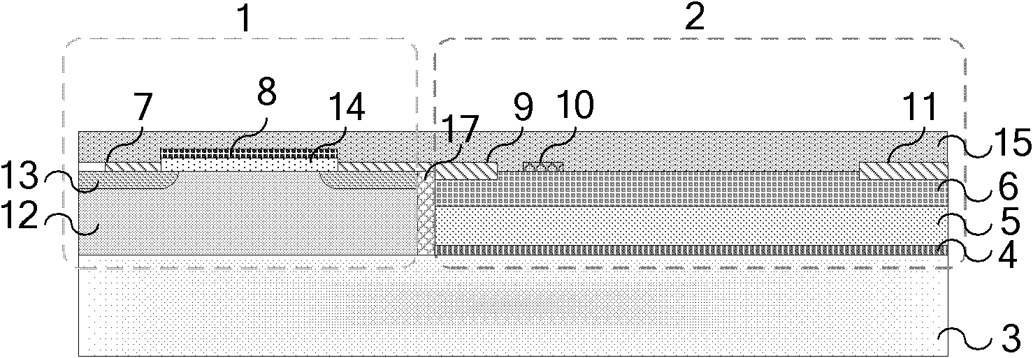
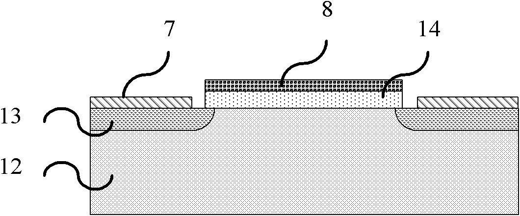
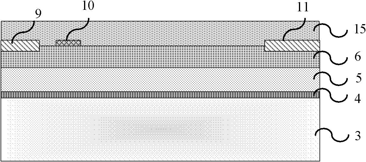
[0021] An enhanced GaN heterojunction field effect transistor based on MOS control, such as figure 1 As shown, it includes a monolithically integrated low-voltage MOS transistor 1 and a depletion-type GaN heterojunction field effect transistor 2 on the same substrate; wherein the drain of the MOS transistor 1 and a depletion-type GaN heterojunction field effect transistor 2 The source of the GaN heterojunction field effect transistor 2 is electrically connected with the gate of the MOS tube 1, or the gate of the GaN heterojunction field effect transistor 2 and the source of the MOS tube 1 are mutually connected. Connected; MOS tube 1 and depletion-mode GaN heterojunction field effect transistor 2 are separated by dielectric isolation trenches.

[0022] In the above scheme:

[0023] 1) The substrate material can be silicon, gallium nitride, silicon carbide or sapphire.

[0024] 2) The material of the dielectric isolation tank is air, SiO 2 , Si 3 N 4 , AlN or A1 2 O 3 .

[0025] 3) Th...


PUM


Abstract

The invention provides an enhanced GaN heterojunction field effect transistor based on metal oxide semiconductor (MOS) control and belongs to the technical field of power semiconductor devices. The enhanced GaN heterojunction field effect transistor comprises a monolithic integrated low-voltage MOS tube and a depletion mode GaN heterojunction field effect transistor, wherein the drain of the MOS tube is connected with the source of the depletion mode GaN heterojunction field effect transistor; the grid of the MOS tube and the grid of the depletion mode GaN heterojunction field effect transistor are connected with each other or the grid of the GaN heterojunction field effect transistor is connected with the source of the MOS tube; and the MOS tube and the depletion mode GaN heterojunction field effect transistor are isolated from each other by using a medium isolation slot. In the enhanced GaN heterojunction field effect transistor based on MOS control, transformation from the depletion mode GaN heterojunction field effect transistor to the enhanced GaN heterojunction field effect transistor is realized by controlling an on/off state of the low-voltage MOS tube connected in series with the depletion mode GaN heterojunction field effect transistor; the enhanced GaN heterojunction field effect transistor has the normally off characteristic of the low-voltage MOS tube and the advantages of high-voltage resistance, low-conductivity resistance and the like of the depletion mode GaN heterojunction field effect transistor, has good frequency characteristic and high output power and density, and is applicable to the high-frequency and high-power fields.

Description

Technical field [0001] The invention belongs to the technical field of power semiconductor devices, and relates to a GaN heterojunction field effect transistor (AlGaN / GaN HFET), in particular to an enhancement mode GaN heterojunction field effect transistor. Background technique [0002] After years of development, silicon (Si)-based power devices have now entered a period of stable performance, and further improvements in their performance are often accompanied by a significant increase in cost. At the same time, many new applications place higher requirements on the size, efficiency, and stability of the power management unit. However, the performance of traditional Si-based power devices has approached its theoretical limit, making wide-bandgap semiconductors an ideal alternative material for power management. As a typical representative of the third generation of semiconductor materials, the wide bandgap semiconductor gallium nitride (GaN) has excellent properties that many ...

Claims


Application Information

Patent Timeline
IPC IPC(8): H01L27/088H01L29/78H01L29/778
Inventor 陈万军魏进汪志刚张竞张波
Owner UNIV OF ELECTRONICS SCI & TECH OF CHINA
Why Eureka
Try Eureka