Gallium-nitride-based light-emitting diode (LED) epitaxial wafer and growth method thereof

A light-emitting diode, gallium nitride-based technology, applied in electrical components, circuits, semiconductor devices, etc., can solve the problems of high acceptor impurity ionization, difficulty, and deviation of growth quality, and achieve the effect of improving growth quality and efficiency.

Inactive Publication Date: 2011-10-05
DALIAN MEIMING EPITAXIAL WAFER TECH
View PDF6 Cites 19 Cited by
  • Summary
  • Abstract
  • Description
  • Claims
  • Application Information

AI Technical Summary

Problems solved by technology

However, the forbidden band width of aluminum gallium nitride is much larger than that of gallium nitride, and the ionization energy of its acceptor impurity is higher, so it is very difficult to obtain a p-type layer with high hole concentration
In addition, the optimum growth temperature of the p-type AlGaN electron bloc

Method used


Image

  • Gallium-nitride-based light-emitting diode (LED) epitaxial wafer and growth method thereof
  • Gallium-nitride-based light-emitting diode (LED) epitaxial wafer and growth method thereof

Examples


Embodiment 1

[0022] Embodiment 1 adopts MOCVD epitaxial growth:

[0023] 1. Put the sapphire substrate with (0001) crystal orientation into the reaction chamber, and then 2 The temperature is raised to 1050°C in the environment, stabilized for 10 minutes, and the substrate is purified at high temperature;

[0024] 2. Lower the temperature to 530°C to grow a low-temperature GaN-based buffer layer with a thickness of 20nm;

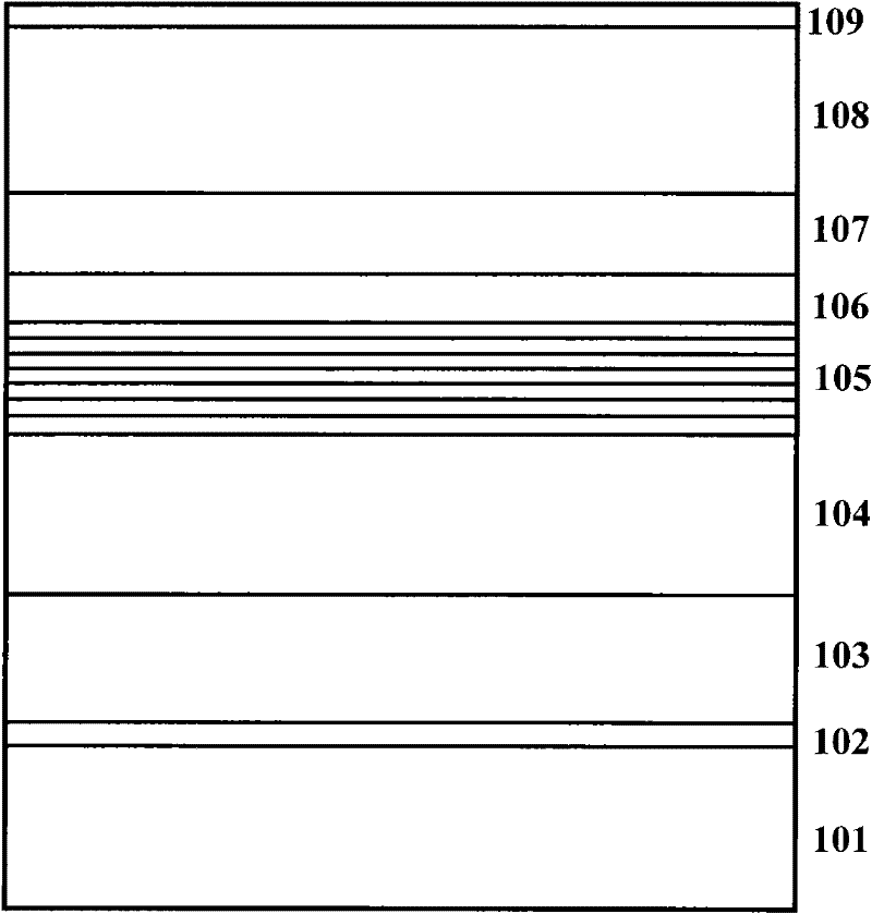
[0025] 3. Raise the temperature to 1100°C to grow a non-doped gallium nitride layer with a thickness of 1 μm;

[0026] 4. Grow an n-type GaN layer with a thickness of 1.5 μm at 1100°C;

[0027] 5. Grow 5 periods of multi-quantum well layers in N2 environment, gallium nitride barrier layer: thickness is 20nm, growth temperature is 850°C; indium gallium nitrogen well layer: thickness is 1.6nm, growth temperature is 810°C;

[0028] 6. Raise the temperature to 900°C to grow a GaN-based p-type hole injection layer with a thickness of 20nm;

[0029] 7. Raise the temperatur...

Embodiment 2

[0035] Embodiment 2 uses MOCVD to grow epitaxial wafers, and grows sequentially from bottom to top:

[0036] 1. Put the sapphire substrate with (0001) crystal orientation into the reaction chamber, and then 2 The temperature is raised to 1250°C in the environment, stabilized for 5 minutes, and the substrate is purified at high temperature;

[0037] 2. Lower the temperature to 540°C to grow a low-temperature gallium nitride-based buffer layer with a thickness of 15nm;

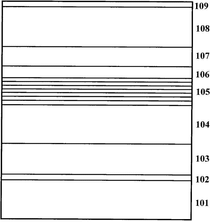
[0038] 3. Raise the temperature to 1150°C to grow a non-doped gallium nitride layer with a thickness of 2 μm;

[0039] 4. Grow an n-type gallium nitride layer with a thickness of 2 μm at 1150°C;

[0040] 5. In N 2 Growth of 15 cycles of multi-quantum well layers in the environment, gallium nitride barrier layer: thickness 13nm, growth temperature 950°C; indium gallium nitrogen well layer: thickness 2nm, growth temperature 830°C;

[0041] 6. Raise the temperature to 1050°C to grow a GaN-based p-type hole inje...

Embodiment 3

[0048] Embodiment 3 uses MOCVD to grow epitaxial wafers, and grows sequentially from bottom to top:

[0049] 1. Put the sapphire substrate with (0001) crystal orientation into the reaction chamber, and then 2 The temperature is raised to 1190°C in the environment, stabilized for 7 minutes, and the substrate is purified at high temperature;

[0050] 2. Lower the temperature to 550°C to grow a low-temperature gallium nitride-based buffer layer with a thickness of 30nm;

[0051] 3. Raise the temperature to 1200°C to grow a non-doped gallium nitride layer with a thickness of 2 μm;

[0052] 4. Grow n-type gallium nitride layer with a thickness of 3 μm at 1200°C;

[0053] 5. In N 2 Growth of 20 cycles of multi-quantum well layers in the environment, gallium nitride barrier layer: thickness 10nm, growth temperature 850°C; indium gallium nitrogen well layer: thickness 2nm, growth temperature 820°C;

[0054] 6. Raise the temperature to 950°C to grow a GaN-based p-type hole injectio...


PUM

PropertyMeasurementUnit
Thicknessaaaaaaaaaa
Thicknessaaaaaaaaaa
Thicknessaaaaaaaaaa

Abstract

The invention discloses a growth method of a gallium-nitride-based epitaxial wafer. In the epitaxial wafer, triethyl gallium used as a metal organic source of gallium and di (cyclopentadienyl) magnesium used as an acceptor impurity growth p-type cavity injection layer are adopted between a multiple quantum well layer and a p-type AlGaN layer; and according to the growth structure, the bulk resistance of the p-type layer is reduced, the effective concentration of the injected cavity is improved, the effective compound of the cavity and an electron in an active region is enlarged, and the luminous efficiency of a light-emitting diode (LED) is improved. According to a standard chip process, a chip which has a size of 300*200 mu m<2> and uses Indium tin oxide (ITO) as a transparent electrode is manufactured, the forward voltage of the chip can be reduced by 0.15V, and the light transmission efficiency is improved by above 17%.

Description

technical field [0001] The invention relates to a gallium nitride-based epitaxial wafer and a growth method thereof, in particular to a p-type gallium nitride-based LED epitaxial wafer with low impedance and high hole concentration and a growth method thereof. technical background [0002] Gallium nitride (GaN)-based compounds are direct bandgap wide-bandgap semiconductors, whose bandgap is continuously adjustable from 1.8-6.2eV, and have a high breakdown voltage, so they are widely used in high-brightness blue-green light-emitting diodes (LED, Light Emitting Diode), blue-violet laser diode (LD, Laser Diode) and high electron mobility field effect transistor (HEMT, High Electron Mobility Transistor). In recent years, high-brightness blue-green LEDs have developed rapidly and have become necessary light-emitting devices for full-color high-brightness large-scale outdoor displays and traffic lights. At the same time, white LEDs made of blue-light LEDs that excite yellow phosph...

Claims


Application Information

Patent Timeline
IPC IPC(8): H01L33/14
Inventor 刘俊杨天鹏王东盛关秋云展望周德保肖志国
Owner DALIAN MEIMING EPITAXIAL WAFER TECH
Why Eureka
Try Eureka