Phase transition storage material and preparation method thereof
A phase-change storage and thin-film preparation technology, applied in the field of phase-change storage materials and their preparation, can solve the problems of poor thermal stability and data retention, slow phase-change speed, environmental pollution, etc., and achieve stable composition shortening and fast crystallization. Speed, simple process effect
- Summary
- Abstract
- Description
- Claims
- Application Information
AI Technical Summary
Problems solved by technology
Method used
Image
Examples
Embodiment 1
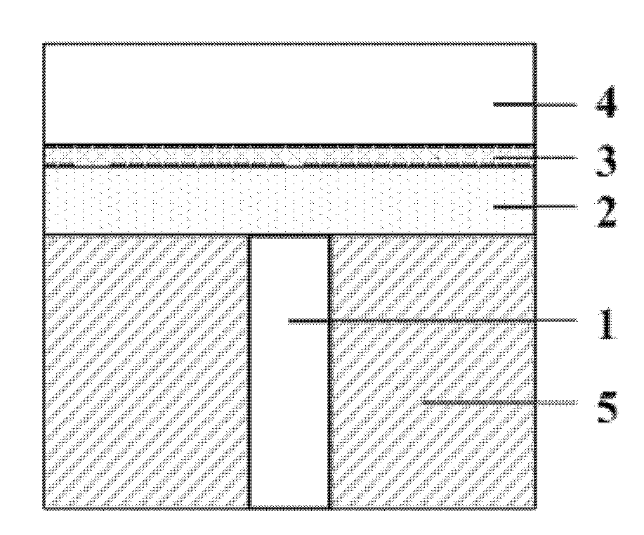
[0031] see figure 1 , a phase-change memory cell with a vertical structure, the phase-change memory cell includes a lower electrode 1, a phase-change memory material layer 2 on the lower electrode 1, a transition layer 3 on the phase-change memory material layer 2, and a transition layer 3 on the transition The upper electrode 4 on the layer 3; the lower electrode 1 is surrounded by an insulating medium 5.
[0032] The phase-change storage material layer 2 is a phase-change thin film material, which is selected from the gallium-antimony-selenium (Ga-Sb-Se) compound provided by the present invention. As a storage medium, it is the core of the phase change memory unit. Wherein, the lower electrode 1 and the upper electrode 4 can be selected from Al, Ti, W, graphite, TiN, Cu, TiW or other conductive materials. The transition layer 3 can be TiN or TaN, and its thickness is about 10-30 nanometers. Preferably 20 nm. The insulating layer 5 can be SiO 2 or Si 3 N 4 Material.
...
Embodiment 2
[0036] Phase-change storage material gallium-antimony-selenium (Ga-Sb-Se) compound provided by the invention, its chemical composition is Ga x Sb y Se z , wherein 4<x<40, 25<y<85, 5<z<70, x+y+z=100.
[0037] When it is used in a phase-change memory unit with a vertical structure, the lower electrode 1 and the upper electrode 4 can be made of Al, Ti, W, graphite, TiN, Cu, TiW or other conductive materials. The transition layer 3 can be TiN or TaN, and its thickness is about 10-30 nanometers. Preferably 20 nm. The insulating layer 5 can be SiO 2 or Si 3 N 4 Material.
[0038] The phase-change storage material Ga-Sb-Se described in the present invention can be prepared by multi-target co-sputtering. Using GaSb alloy target and Sb 2 Se 3 (or Sb x Se, 1-4 Pascal, the sputtering pressure is 0.18 Pascal to 0.25 Pascal, the sputtering gas is argon, the temperature is room temperature, the RF power applied to the GaSb alloy target is 10 watts to 45 watts, applied to the Sb ...
Embodiment 3
[0040] Preferably, the phase change storage material gallium-antimony-selenium (Ga-Sb-Se) compound provided by the present invention has a chemical composition of Gax Sb y Se z , wherein, 10≤x≤20, 50≤y≤85, 20≤z≤40, x+y+z=100.
[0041] The present invention also includes a preparation method of a phase-change memory material, the preparation method comprising any one of the following methods: (1) using a GaSb alloy target and a Sb x Magnetron co-sputtering of two Se alloy targets, where 12 Se 3 Co-sputtering with Sb three-target magnetron.
PUM
 Abstract
Description
Claims
Application Information


