Method for improving interface caking property of dye sensitized solar cell substrate

A solar cell and dye sensitization technology, applied in the field of solar cell utilization, can solve the problem of poor interface adhesion between connecting nano-thin film photoelectrode and conductive substrate, lower distribution quality of upper semiconductor nanocrystalline thin film, lower electron transport performance and collection efficiency and other problems, to achieve the effect of maintaining good network structure morphology, stable performance of photoelectrode materials, and good processing effect

Active Publication Date: 2012-01-18
XI'AN UNIVERSITY OF ARCHITECTURE AND TECHNOLOGY
View PDF2 Cites 0 Cited by
  • Summary
  • Abstract
  • Description
  • Claims
  • Application Information

AI Technical Summary

Problems solved by technology

These defects lead to the poor connectivity between the particles that make up the nano-film and the interface adhesion between the nano-film photoelectrode and the conductive substrate, which makes the conductive substrate easy to directly contact with the electrolyte, increases the chance of electronic recombination, and reduces the electron density. Transmission Performance and Collection Efficiency
In addition, these defects also lead to a decrease in the distribution quality of the semiconductor nanocrystal film per unit area, reducing the adsorption amount of dye molecules.

Method used


Image

  • Method for improving interface caking property of dye sensitized solar cell substrate
  • Method for improving interface caking property of dye sensitized solar cell substrate
  • Method for improving interface caking property of dye sensitized solar cell substrate

Examples


preparation example Construction

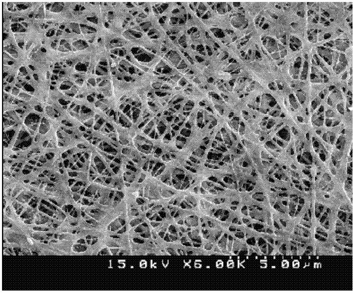
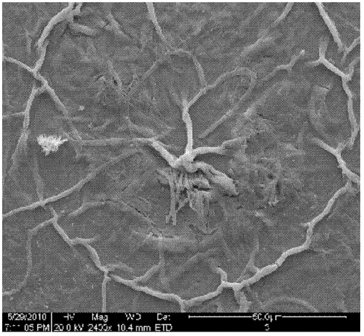
[0060] 3) Preparation of ZnO precursor polymer gel:

[0061] The hydrated salt of zinc (Zn(CH 3 COO) 2 2H 2 O, ZnSO 4 ·7H 2 O or Zn(NO 3 ) 2 ·6H 2 One in O), polymer (one in PVAc, PVA or PVP), solvent (one or two in DMF, deionized water or ethanol) and catalyst (acetic acid, add or not add) press Put the ratio listed in the table into the beaker, or further add dopant (Al(NO 3 ) 3 9H 2 O, Al 2 (SO 4 ) 3 ·xH 2 O, AlCl 3 ·6H 2 One of O, added or not), heated to 60°C; at a speed of 240-400r / min, magnetically stirred for 6hrs to obtain a uniform and transparent ZnO precursor polymer gel. The ZnO precursor polymer gel is formulated according to the raw materials in the following table 1 parts by weight:

[0062] Table 1 Raw material composition weight parts of ZnO precursor polymer gel (unit: gram)

[0063]


PUM

PropertyMeasurementUnit
thicknessaaaaaaaaaa

Abstract

The invention discloses a method for improving the interface caking property of a dye sensitized solar cell substrate. The method comprises the following steps of: 1, cleaning FTO (Fluorine or antimony doped Tin Oxide) conductive glass; annealing the FTO conductive glass; 3, preparing ZnO precursor polymer gel; 4, conducting a ZnO nano fiber film stress buffer layer; 5, autoclaving and annealing the ZnO nano fiber film stress buffer layer; 6, preparing a ZnO nano fiber film photoelectrode; and 7, constructing a nano fiber film dye sensitized solar cell (DSSC). The stress buffer layer constructed in the method can effectively release thermal stress generated between a nano fiber film working electrode and a conductive substrate, prevents the sintered ZnO nano fiber film working electrode from cracking and being broken and the working electrode from being stripped from the substrate, effectively improves the caking property of the ZnO nano fiber film working electrode and the conductive substrate, further improves the stability of the working electrode, increases photoelectric energy conversion efficiency of the DSSC, prolonging the service life of the DSSC, and has important application and popularization values.

Description

technical field [0001] The invention belongs to the technical field of solar cell utilization, and in particular relates to an effective method for improving the interface adhesion between a photoelectrode of a dye-sensitized ZnO nanofiber thin film solar cell and a conductive substrate. Background technique [0002] As a way to utilize solar energy, solar cells have developed rapidly since the 1990s. In the 20th century, with the rapid development of photovoltaic technology, solar energy utilization technology is fundamentally changing the way of energy production, supply and consumption. However, the development of traditional silicon solar cells is limited by the limitation of conversion efficiency and the shortage of raw materials. Although thin-film and concentrating solar cells have entered commercial mass production, only a few manufacturers can produce them. In addition, due to the low conversion efficiency and the increase in investment in production line equipment...

Claims


Application Information

Patent Timeline
Patent Type & Authority Applications(China)
IPC IPC(8): H01G9/04H01G9/20H01M14/00H01L51/44H01L51/48
CPCY02E10/542Y02E10/549
Inventor 云斯宁
Owner XI'AN UNIVERSITY OF ARCHITECTURE AND TECHNOLOGY
Why Eureka
Try Eureka