Method for manufacturing three-dimensional silicon mold directly bonded by low-temperature plasma activation

A direct bonding, plasma technology, applied in gaseous chemical plating, fabrication of microstructure devices, processes for producing decorative surface effects, etc. , micro-mold is difficult and other problems, to achieve the effect of less pollution, enhanced stability and high controllability

Inactive Publication Date: 2012-05-02
HUAZHONG UNIV OF SCI & TECH
View PDF5 Cites 8 Cited by
  • Summary
  • Abstract
  • Description
  • Claims
  • Application Information

AI Technical Summary

Problems solved by technology

Due to the very small size of the micro-mold in the micro-forming process, the design, manufacture and material selection of the mold have changed, and the traditional mold design principles cannot be fully applied to the micro-scale; correspondingly, the processing of the micro-mold has been difficult to use the traditional CNC machining, EDM and other means
The currently used special processing methods such as LIGA have high cost and low efficiency, and are not satisfactory in processing complex three-dimensional cavities and controlling surface roughness.

Method used


Image

  • Method for manufacturing three-dimensional silicon mold directly bonded by low-temperature plasma activation
  • Method for manufacturing three-dimensional silicon mold directly bonded by low-temperature plasma activation
  • Method for manufacturing three-dimensional silicon mold directly bonded by low-temperature plasma activation

Examples


Embodiment 1

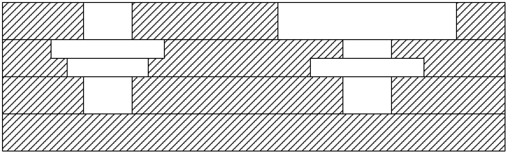
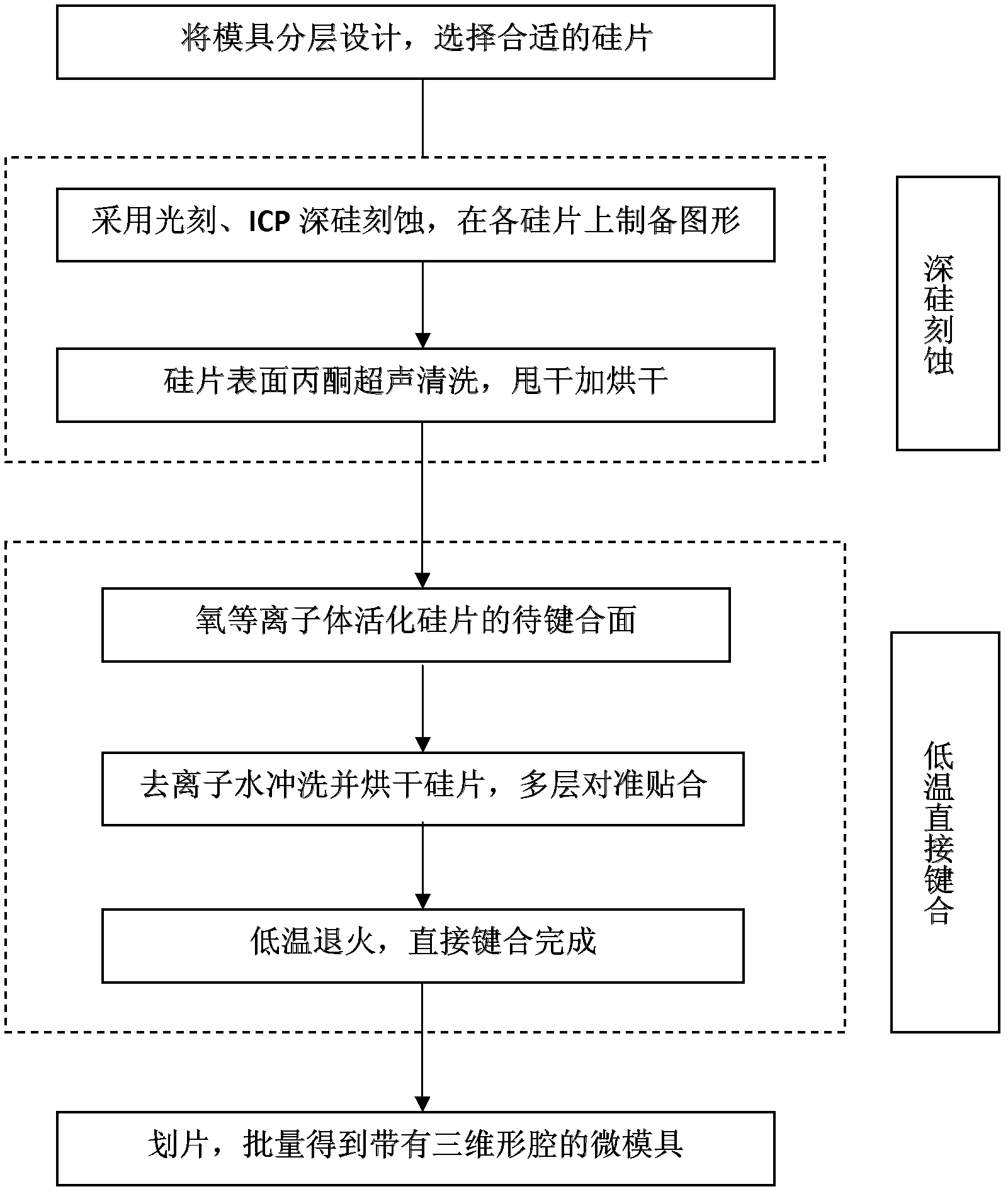
[0026] figure 1 For the mold of the three-dimensional micro-parts to be prepared in this embodiment, figure 2 Realize the process flow chart of this mold for the present invention. Divide the part into 4 layers in the Z direction, select 4 silicon wafers of corresponding thickness, the middle two layers of silicon wafers are double-thrown silicon wafers, and the top and bottom silicon wafers are single-thrown silicon wafers.

[0027] The method of photolithography and ICP (inductively coupled plasma) deep silicon etching is used for each layer of silicon wafers, and the structural patterns of the corresponding layers of the parts to be prepared are accurately etched. The first and third layers of silicon wafers are etched through at one time. The second layer of silicon wafer requires photolithography and ICP etching on the front and back sides to realize the stepped cavity in the silicon wafer; the photolithography and ICP deep silicon etching process is: uniform glue on th...

Embodiment 2

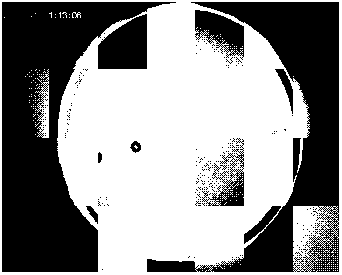
[0034] image 3 It is the effect diagram of low-temperature plasma activation of silicon-silicon double-layer direct bonding, and its process steps:

[0035] The newly shipped 2-inch silicon wafers are not wet-cleaned, but are directly cleaned and activated by oxygen plasma, with a flow rate of 50sccm, a radio frequency power of 150W, and an activation time of 20s; each silicon wafer after activation is rinsed with deionized water for 3 minutes , spinning and drying plus drying, lamination of silicon wafers;

[0036] Anneal the laminated multi-layer silicon wafer at a temperature of 160°C for 72 hours to complete the double-layer direct bonding of the silicon wafer.

Embodiment 3

[0038] Figure 4 It is the effect diagram of direct bonding of three layers of silicon wafers

[0039] The materials are 2 pieces of 2-inch silicon wafers with single throwing and 1 piece of 2-inch silicon wafers with double throwing;

[0040] The newly shipped 2-inch silicon wafers are not wet-cleaned, but are directly cleaned and activated by oxygen plasma. One polished surface of all wafers is activated once, and the other side of double-polished wafers is activated twice. The plasma equipment used is domestic ME-RIE, the surface activation atmosphere is oxygen flow rate 100sccm, radio frequency power 100W, activation time 5s;

[0041] Rinse each silicon wafer after activation with deionized water for 3 minutes, spin dry and dry, and align and bond all silicon wafers in order from top to bottom (double-polished silicon wafers are in the middle layer);

[0042] Anneal the laminated multi-layer silicon wafers at a temperature of 300°C for 12 hours to complete the multi-lay...


PUM


Abstract

The invention provides a method for manufacturing a three-dimensional silicon mold directly bonded by low-temperature plasma activation. The method comprises the following steps of: designing a micro-mold to be manufactured in the Z direction in a laminated manner; selecting silicon chips with appropriate thicknesses as substrates on all layers, and accurately etching the silicon chips on all the layers by a photoetching or inductively-coupled plasma (ICP) deep silicon etching method to form a structural graphic of a mold corresponding layer; cleaning the surfaces of all the silicon chips, performing plasma activation, pre-bonding, and annealing at a low temperature to finish the direct bonding of a plurality of layers of silicon chips; and finally, scribing to acquire three-dimensional micro silicon molds in batches. The method is suitable for efficiently manufacturing the silicon mold with a stepped high depth-to-width ratio three-dimensional micro structure (such as a micro gear shaft, a micro stepped shaft, a micro pump and the like) in a microelectromechanical system (MEMS) device at high accuracy.

Description

technical field [0001] The invention belongs to the field of semiconductor direct bonding and MEMS packaging, and relates to mold manufacturing technology, in particular to a manufacturing method of a three-dimensional micro-mold, specifically a preparation method for realizing silicon-silicon direct bonding through low-temperature plasma activation. Background technique [0002] In recent years, communications, computers, automotive electronics, defense technology and other consumer products have put forward higher requirements for microelectronic packaging, that is, smaller, thinner, lighter, multi-functional, high reliability, low power consumption and low cost . At the same time, with the development of the miniaturization trend of scientific and technological products, the demand for components such as microprocessors and micro-executions in MEMS devices is increasing. more extensive. [0003] In actual production, there is an increasing demand for micro-components, w...

Claims


Application Information

Patent Timeline
Patent Type & Authority Applications(China)
IPC IPC(8): B81C1/00
Inventor 廖广兰卓锐史铁林聂磊张昆
Owner HUAZHONG UNIV OF SCI & TECH
Why Eureka
Try Eureka