

Cathode injection material, and manufacturing method and application thereof
A cathode injection and cesium salt technology, applied in the field of electric light sources, can solve the problems of difficult electron injection, sensitivity, and high work function, and achieve the effects of enhanced electron injection efficiency, easy acquisition, and low cost
- Summary
- Abstract
- Description
- Claims
- Application Information
AI Technical Summary
Problems solved by technology
Method used
Image

Examples
preparation example Construction
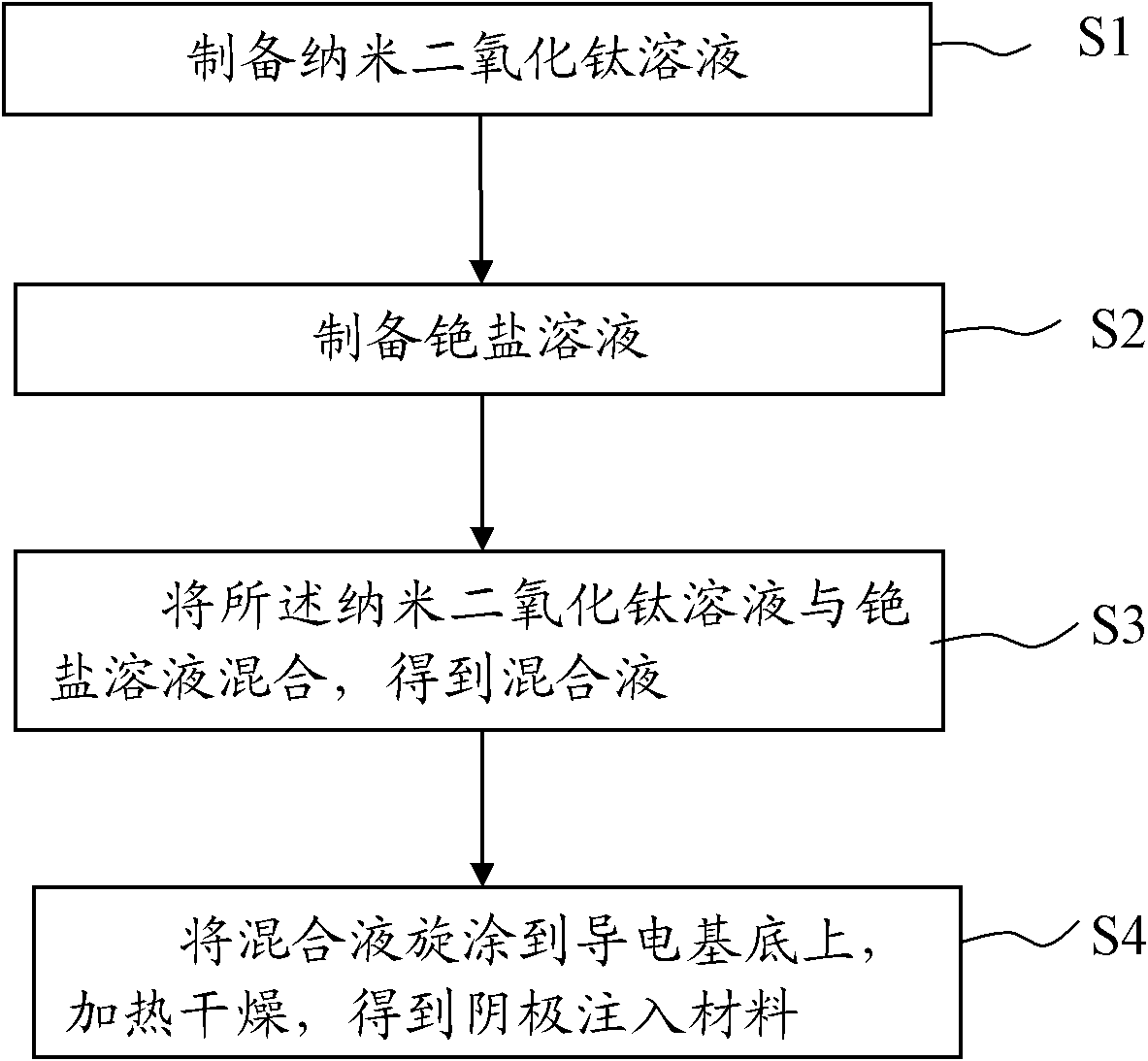
[0031] The embodiment of the present invention also provides the preparation method of the cathode injection material, such as figure 1 As shown, the method includes the following steps:
[0032] S1: preparing a nano-titanium dioxide solution, mixing the nano-titanium dioxide with an alcohol solvent or / and double distilled water to prepare a nano-titanium dioxide solution with a mass concentration of 0.1-2%;
[0033] S2: preparing a cesium salt solution, mixing the cesium salt with an alcohol or ether solvent to prepare a cesium salt solution with a mass concentration of 0.1-2%;
[0034] S3: mixing the nano-titanium dioxide solution with the cesium salt solution to obtain a mixed solution;
[0035] S4: Spin-coat the mixed solution on the conductive substrate, heat and dry to obtain the cathode injection material.
[0036] The preparation method of the above-mentioned cathode injection material only needs to mix the nano-titanium dioxide and cesium salt, coat it on the substr...
Embodiment 1
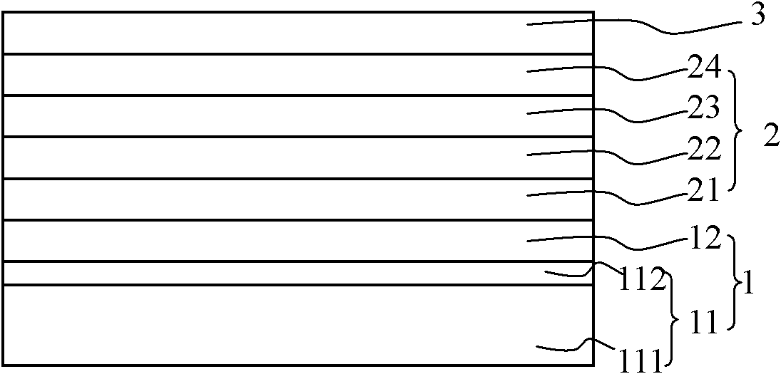
[0060] The structure of the organic electroluminescent device of this embodiment is as follows figure 2 As shown, the organic electroluminescent device includes an organic electroluminescent device cathode 1, and an electron transport layer 21, a light-emitting layer 22, a hole transport layer 23, and a hole injection layer 24 that are sequentially combined with the organic electroluminescent device cathode 1 and anode 3. Wherein, the cathode 1 of the organic electroluminescent device includes a conductive substrate 11 and a cathode injection layer 12 bonded on the surface of the conductive substrate 11 .
[0061] The above-mentioned conductive substrate 11 is indium tin oxide glass (ITO glass), the thickness of the cathode injection layer 12 is 50nm, the electron transport layer 21 is a 50nm thick PBD layer, and the light emitting layer 22 is a 70nm thick AlQ 3 layer, the hole transport layer 23 is a 40nm thick TPD layer, and the hole injection layer is 2410nm thick MoO 3 La...
Embodiment 2
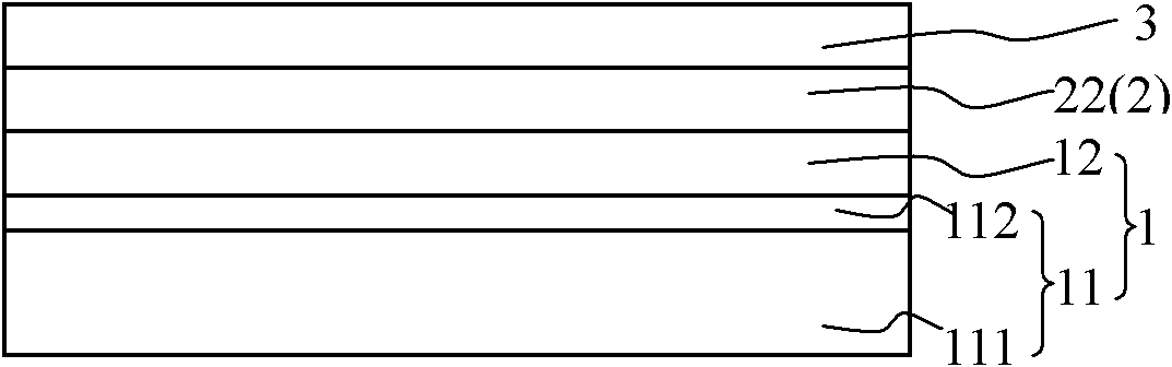
[0075] The organic electroluminescence device structure of this embodiment is the same as embodiment 1 and figure 2 shown. Its preparation method is as follows:
[0076] (1) Photolithographically process the ITO glass, cut it into the required light-emitting area, and then use detergent, deionized water, acetone, ethanol, and isopropanol to ultrasonically clean it for 15 minutes, and then perform oxygen plasma treatment on it , the oxygen plasma treatment time is 5min, and the power is 50W, to reduce the roughness and contact angle of the conductive glass surface, improve the wettability and adsorption of the surface, remove the organic pollutants on the conductive glass surface, and prepare the conductive substrate 11;
[0077] (2) Preparation of cathode injection material:
[0078] (21) Commercially available TiO with a particle size of 20nm 2 Particles and absolute ethanol were formulated into a solution with a mass fraction of 0.2%, and the solvent was added dropwise w...
PUM
| Property | Measurement | Unit |
|---|---|---|
| Thickness | aaaaa | aaaaa |
| Thickness | aaaaa | aaaaa |
| Thickness | aaaaa | aaaaa |
Abstract
Description
Claims
Application Information