Eureka AIR delivers breakthrough ideas for toughest innovation challenges, trusted by R&D personnel around the world.

Cu-Al alloy powder, alloy paste utilizing same, and electronic component

A technology of alloy powder and electronic components, applied in printed circuit parts, electrical components, electric solid devices, etc., can solve the problems of weather resistance deterioration, material cost increase, electronic component products are not applicable, etc., and achieve migration resistance Excellent effect of suppressing air bubbles

Inactive Publication Date: 2012-05-23
HITACHI CHEM CO LTD
View PDF7 Cites 14 Cited by
  • Summary
  • Abstract
  • Description
  • Claims
  • Application Information

AI Technical Summary

Problems solved by technology

However, it is pointed out that when one or more elements selected from the group consisting of Al, Au, Ag, Ti, Ni, Co, and Si are added to this alloy in a total of 3.0 wt% or more, the weather resistance deteriorates on the contrary.
In addition, there is a problem that since the addition of Mo is necessary, the material cost increases, so it is not suitable for electronic parts products with low market cost.

Method used


Image

  • Cu-Al alloy powder, alloy paste utilizing same, and electronic component
  • Cu-Al alloy powder, alloy paste utilizing same, and electronic component
  • Cu-Al alloy powder, alloy paste utilizing same, and electronic component

Examples


Embodiment 1

[0064] This example shows an example of controlling the crystal particle size distribution of Cu—Al alloy powder, which is important for cost reduction in the manufacturing process of forming electrodes, wiring, and / or contact members of electronic components. In the present invention, in the Cu-Al alloy powder manufacturing process of melting of the above-mentioned Cu-Al alloy, powderization by nozzle spraying, drying of the powder, classification of the powder, mixing of the classified powder, and deoxidation-dehydration, Cu - Al alloy powder (spherical) particle size distribution of the maximum diameter of 30 μm or less, the average particle size of the alloy powder is 5 μm or less, then the yield of the raw material into the alloy dissolved in more than 90%. An example of the particle size distribution of the Cu-Al alloy powder at this time is shown in Figure 11 . In addition, the flaky Cu-Al alloy powder is manufactured from the above-mentioned powder using a ball mill, e...

Embodiment 2

[0068] In the Cu-Al alloy powder manufacturing process of melting of Cu-Al alloy by nozzle spraying, drying of powder, classification of powder, mixing of classified powder, and deoxidation-dehydration of Cu-Al alloy powder of the present invention, this example shows An example of a classification method implementing Cu-Al alloy powder particle size distribution control. First, as an example of wet classification, the present embodiment in which classification is carried out by a low-cost natural sedimentation method is used as follows. The present invention produced by the method includes melting of the Cu-Al alloy related to the present invention, powderization by nozzle spraying, drying of the powder, classification of the powder, mixing of the classified powder, and deoxidation-dehydration steps. Cu-Al alloy powder particles (Al: 8wt%, density 8.4g / cm 3 ) 200g, surfactant polyacrylic acid to 0.8wt% of particles, and pure water to 1000g, put into polymerization container....

Embodiment 3

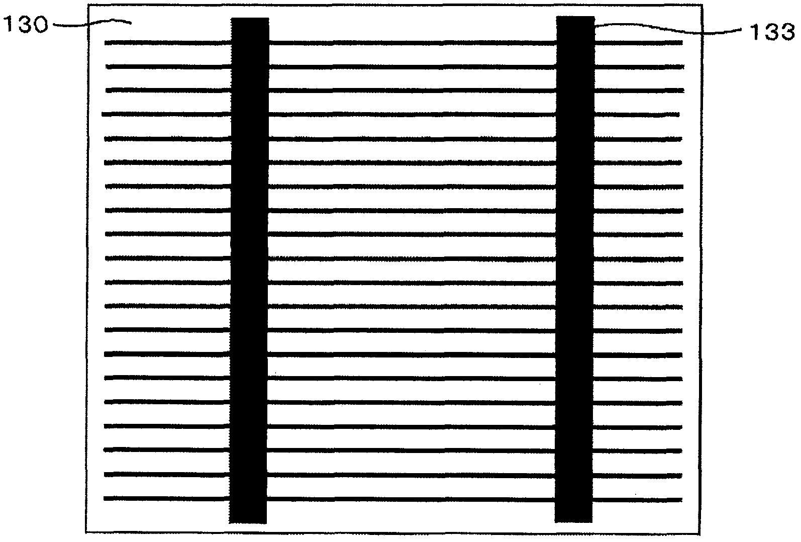
[0071] An example in which the electrode of the present invention is used in the double-sided electrode crystalline silicon (Si) solar cell element of the present invention will be described. A cross-sectional view of a typical solar cell element, and an outline of the light-receiving surface and the back surface are shown in figure 2 , image 3 and Figure 4 .

[0072] Generally, single crystal or polycrystalline Si or the like is used for the semiconductor substrate 130 of the solar cell element. The semiconductor substrate 130 contains boron or the like, and forms a p-type semiconductor. On the light-receiving side, unevenness is formed by etching to suppress reflection of sunlight. This light-receiving surface is doped with phosphorus or the like to form an n-type semiconductor diffusion layer 131 with a thickness of nanometers, and at the same time, a pn junction is formed at the boundary with the p-type entire portion. In addition, an antireflection layer 132 made ...


PUM

PropertyMeasurementUnit
thicknessaaaaaaaaaa
particle sizeaaaaaaaaaa

Abstract

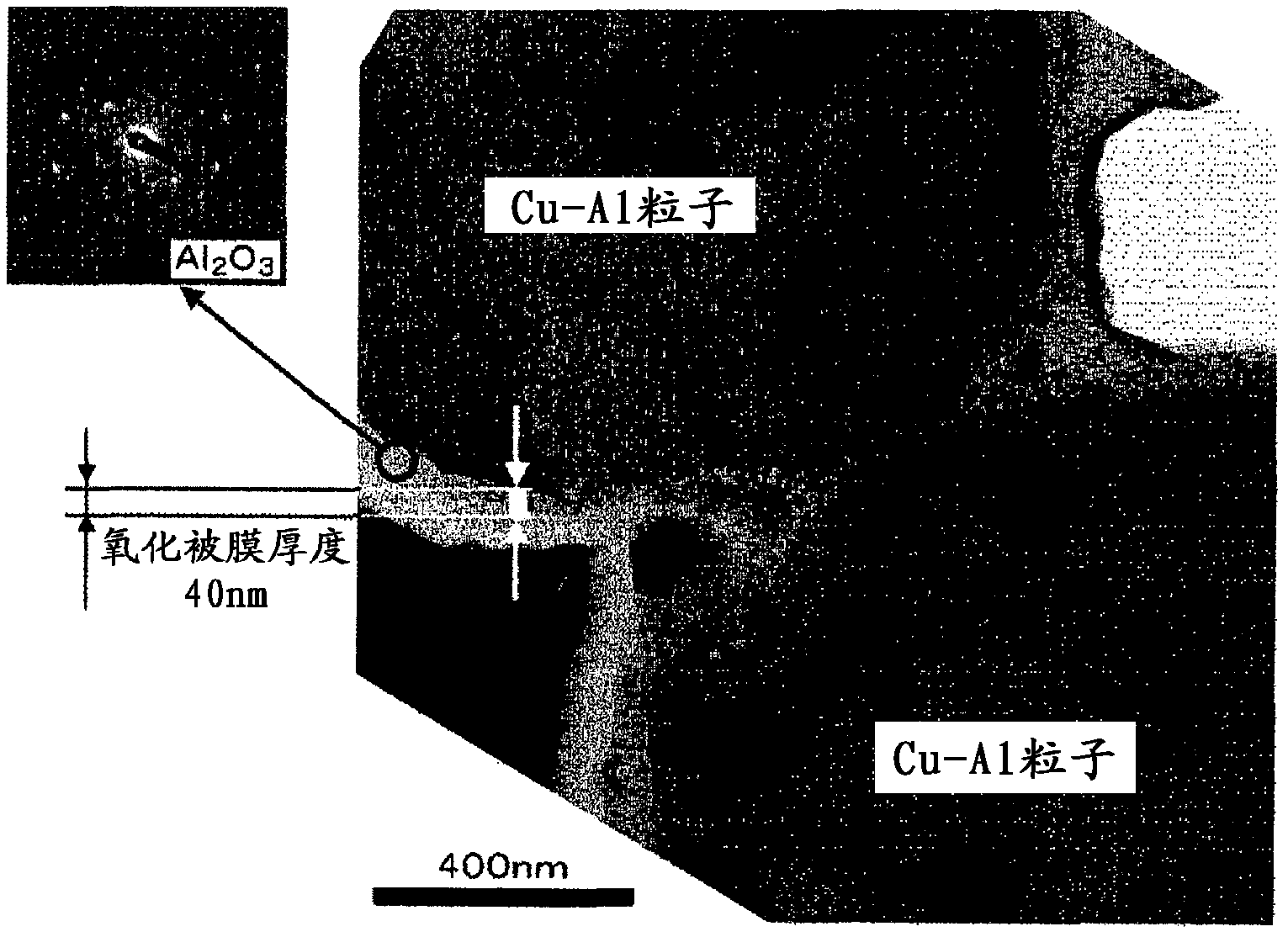
Disclosed is an electronic component wherein wiring and electrodes are produced by baking a paste, and which has wiring that connects to a glass or glass ceramic member. The electronic component can suppress an increase in electrical resistance resulting from oxidation, can suppress the generation of air bubbles in the glass or glass ceramic, and uses a Cu wiring material with excellent migration resistance. Further disclosed is a Cu-Al alloy powder that comprises Cu and preferably no more than 50 mass % of Al, and that is characterized by the surface of the aforementioned Cu-Al alloy powder being covered by an Al oxide coat layer with a thickness of no more than 80 nm. This powder is combined with a glass or a glass ceramic material to form a paste, and can be used to form wiring, electrodes, and / or contact members.

Description

technical field [0001] The present invention relates to a copper-based wiring, electrode and / or contact wiring material capable of suppressing oxidation of wiring materials in the manufacture of wiring, electrodes and / or contacts, and an electronic component using the same for wiring. Background technique [0002] Electronic components with wiring, electrodes, and / or contacts, etc., are manufactured using a manufacturing process that does not come into contact with an oxidizing atmosphere, as represented by LSI wiring, pure Cu can be used as wiring or electrode materials . On the other hand, as used in a typical manufacturing process such as a large plasma display device, metal wiring is buried in a glass dielectric, and in the manufacturing process, it is carried out in an oxidizing atmosphere, for example, at a high temperature range of 400°C or higher. heat treatment. [0003] In addition, in an electrode for a solar cell, heat treatment (baking) is performed in an atmo...

Claims


Application Information

Patent Timeline
Patent Type & Authority Applications(China)
IPC IPC(8): B22F1/02H01B1/22H01B5/00H01J11/20H01L21/28H01L21/288H01L21/3205H01L23/52H01L31/04H05K1/09B22F1/068B22F1/107B22F1/16H01J11/12H01J11/22H01J11/24H01J11/26H01J11/34H01L21/768H01L23/532
CPCH05K1/092H01L2924/09701H05K2203/0315C22C1/0425H01B1/026H01J11/12H01L21/4867H01J2211/225B22F1/0074H01L23/49883H05K2201/0224Y02E10/50H01L2924/0002B22F1/02H01L31/022425C22C1/05B22F1/0055H01J11/22H05K3/4629B22F1/068B22F1/107B22F1/16H01L2924/00H01B1/22H01B5/00H01L21/28
Inventor 加藤隆彦内藤孝青柳拓也山本浩贵吉田诚人片寄光雄武田信司田中直敬足立修一郎
Owner HITACHI CHEM CO LTD
Why Eureka
Eureka Blog
Learn More