Method for detecting two dimensional nanostructured material film surface detect

A two-dimensional nanostructure, material thin film technology, applied in the direction of material analysis using measurement of secondary emissions, optical testing flaws/defects, etc., can solve the problems of long cycle, complex operating procedures, limited probe scanning range, etc.

Inactive Publication Date: 2012-06-13
PEKING UNIV
View PDF3 Cites 35 Cited by
  • Summary
  • Abstract
  • Description
  • Claims
  • Application Information

AI Technical Summary

Problems solved by technology

Defects on the surface of two-dimensional material films have a significant impact on its physical or chemical properties, and can even significantly change some properties. For example, ideal graphene should be hydrophobic, but surface defects can cause graphene to have a strong resistance to water. Adsorption, so that the graphene containing defects is weakly hydrophobic or even hydrophilic
Among them, although the Raman spectrometer can detect the existence of defects more sensitively, it is a statistical result that cannot accurately determine the location and distribution of defects.
However, STM and AFM determine defects by characterizing the surface topography of materials, which can characterize precise point defects and their positions, but the scanning range of the probe is limited (within hundreds of microns), and due to the scanning of the probe, the speed is relatively slow , the cycle is longer, in addition, STM requires an ultra-high vacuum environment, the working conditions are harsh, and the operation process is complicated
Optical microscopy can detect partial defects quickly and in a large area, but the premise is that the defects must have optical contrast, such as macroscopic wrinkles, or the boundaries of atomic thickness can be resolved with the help of other contrast materials, but limited to the resolution of optical microscopy (micrometer scale), it is difficult to detect atomic scale steps, lattice defects or boundaries with pure optical microscopy

Method used


Image

  • Method for detecting two dimensional nanostructured material film surface detect
  • Method for detecting two dimensional nanostructured material film surface detect
  • Method for detecting two dimensional nanostructured material film surface detect

Examples


Embodiment 1

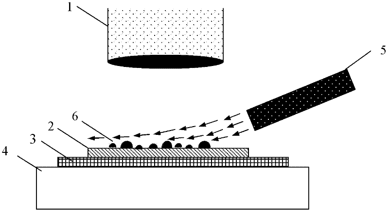
[0041] 1) Select highly oriented graphite (HOPG) with a smooth surface, and use adhesive tape to cleave the surface of the highly oriented graphite to obtain a fresh cleaved surface.

[0042] 2) Fix the highly oriented graphite on a glass slide, put it into an oven, and dry it under the protection of argon at 120°C for 1 hour. After cooling to room temperature, take out the sample and quickly seal it in a desiccator.

[0043] 3) Use a constant temperature tank to heat deionized water to 65°C and maintain a constant temperature; fix the water vapor nozzle on the side of the stage, and adjust the angle between the nozzle and the stage to a suitable value so that the airflow does not cause the sample to move. At the same time, the mixed gas of water vapor can fully contact the surface of the sample.

[0044] 4) Fix the highly oriented graphite in the desiccator above the stage. The focusing optical microscope makes the surface of the sample image clearly, and the CCD video is tu...

Embodiment 2

[0049] 1) Graphite flakes with tens of layers of atomic layer thickness are selected as two-dimensional film materials. The preparation of graphite flakes can be obtained by cleaving graphite films with adhesive tape, and then transferred to SiO 2 Surface (below it is Si, usually expressed as SiO 2 / Si).

[0050] 2) SiO that will support graphite flakes 2 / Si slices were fixed on glass slides with adhesive tape, and then dried under nitrogen protection at 140°C for 1 hour. After cooling to room temperature, the samples were taken out and quickly sealed in a desiccator.

[0051] 3) Heating the deionized water to 70°C and maintaining a constant temperature, adjusting the position of the water vapor nozzle on the stage and the angle of the nozzle on the stage plane.

[0052] 4) Fix the graphite flake sample in the desiccator above the stage; focus the optical microscope to image the sample surface clearly, and turn on the CCD video.

[0053] 5) Nitrogen gas is passed into the ...

Embodiment 3

[0057] 1) Single-layer and double-layer graphene are used as two-dimensional materials to be detected. This thin film material can be obtained by cleaving HOPG once or multiple times, and then transferred to SiO 2 Surface (below it is Si, usually expressed as SiO 2 / Si).

[0058] 2) SiO attached to graphene 2 / Si slices were fixed on glass slides, then dried under the protection of argon at 130°C for 1 h, cooled to room temperature and stored in a desiccator for detection.

[0059] 3) Heat the deionized water to 60°C and keep the temperature constant, fix the steam nozzle at a suitable position on the stage, and adjust the direction of the nozzle and the angle of the stage plane.

[0060] 4) Fix the cooled graphene on the stage, focus the optical microscope to image the sample surface clearly, and turn on the CCD video recording.

[0061] 5) Open the argon throttle valve, spray the mixed gas of water vapor and argon along the graphene surface, and control the flow rate of t...


PUM

PropertyMeasurementUnit
thicknessaaaaaaaaaa

Abstract

The invention discloses a detection method of two dimensional nanostructured material film surface detect distribution and relates to the field of material surface defect and its distribution detection. The method comprises the following steps of: firstly drying a sample beforehand, removing water molecules on the surface of the sample, allowing a gas mixture of steam and other gases to flow on the surface of the sample by a steam injection device, carrying out condensation operation, acquiring morphological, distribution and quantitative features of droplets on the surface of the film material under single and multiple condensation conditions, and determining distribution law of the sample surface defect. As the absorption and condensation process of the water molecules on the surface ofthe two dimensional film material is usually completed in milliseconds, the defect detection is very rapid; in addition, deionized water vapor which is mild is used on the surface of the material, and the sample can be restored to the original state just by a subsequent drying step. Therefore, the method is lossless for the sample to be detected.

Description

technical field [0001] The invention relates to the field of detection of material surface defects and their distribution, in particular to a detection method for the distribution of defects on the surface of two-dimensional nanostructure materials. Background technique [0002] Two-dimensional materials are usually in the shape of a thin film, assuming that the dimensions of the film in the three-dimensional direction are L x , L y and L z , if the size of a certain two directions (for example: L x , L y ) are greater than the Fermi wavelength of the material (λ F ), while the scale in a certain direction (for example: L z ) is less than or equivalent to its Fermi wavelength (λ F ), then this material is a two-dimensional material. The thickness of two-dimensional material films can be below 100 nanometers, and the thinnest can be at the thickness of a single atom. The common one is a layered crystal structure. Since the lattice has dense interatomic forces in the h...

Claims


Application Information

Patent Timeline
Patent Type & Authority Applications(China)
IPC IPC(8): G01N21/88G01N23/22
Inventor 郭剑魏芹芹魏子钧赵华波傅云义黄如张兴
Owner PEKING UNIV
Why Eureka
Try Eureka