Method for preparing metallized ceramic substrate by low-temperature sintering

A metallized ceramic and low-temperature sintering technology, which is applied in the field of electronic manufacturing, can solve the problems of low bonding strength, slow deposition speed, and low reliability, and achieve the effects of small thermal stress, low production cost, and high substrate performance

Inactive Publication Date: 2012-06-20
HUAZHONG UNIV OF SCI & TECH
View PDF3 Cites 33 Cited by
  • Summary
  • Abstract
  • Description
  • Claims
  • Application Information

AI Technical Summary

Problems solved by technology

However, there are also some shortcomings in the DPC substrate: 1) The thickness of the electroplating deposited copper layer is limited, the deposition speed is slow, and the pollution of electroplating waste liquid is large; 2) The bonding strength between metal copper and ceramics is low, and the reliability of the product is low in application.

Method used


Image

  • Method for preparing metallized ceramic substrate by low-temperature sintering
  • Method for preparing metallized ceramic substrate by low-temperature sintering
  • Method for preparing metallized ceramic substrate by low-temperature sintering

Examples


Embodiment 1

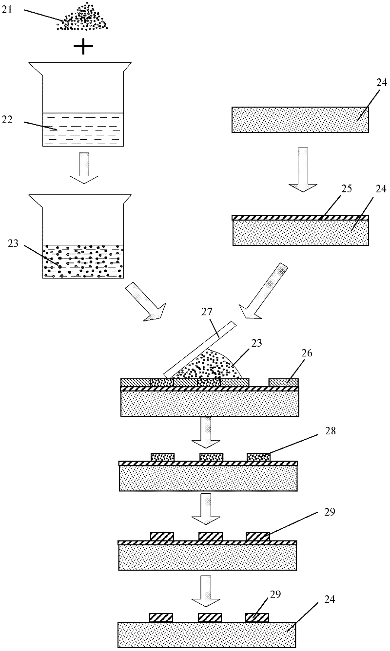
[0017] Material preparation: copper powder: particle size 5-30nm, spherical in appearance; organic compound formula (mass ratio): 5% ethyl cellulose, 1% triethanolamine, fully dissolved with the balance of terpineol.

[0018] The production process is:

[0019] (1) Mix and stir the nano-copper powder and the organic matter in a mass ratio of 70:30 to make a nano-copper paste;

[0020] (2) Metallization of ceramic sheets: Ultrasonic cleaning of 96% alumina substrates with acetone for 10 minutes, and drying; using a multi-target sputtering machine to deposit 30nm titanium films and 50nm copper films on alumina ceramic sheets;

[0021] (3) Printing and coating conductor patterns: using a stainless steel orifice plate and a manual screen printing machine to form nano-copper paste patterns on the alumina substrate; dry at 100°C for 30 minutes to obtain a copper paste layer with a thickness of 100 microns;

[0022] (4) Sintering: Place the alumina ceramic substrate with copper past...

Embodiment 2

[0027] Material preparation: copper powder: particle size 2-20nm, spherical appearance; organic formula (mass ratio): 8% ethyl cellulose, 2% triethanolamine, fully dissolved with the balance of terpineol.

[0028] The production process is:

[0029] (1) Mix and stir the nano-copper powder and the organic matter in a mass ratio of 80:20 to prepare a nano-copper paste;

[0030] (2) Metallization of ceramic sheets: ultrasonically clean the aluminum nitride substrate with acetone for 10 minutes, and dry it; use a multi-target sputtering machine to deposit a 20nm titanium film and a 50nm copper film on the aluminum nitride ceramic sheet;

[0031] (3) Printing and coating conductor graphics: using a stainless steel orifice plate and a manual screen printing machine to prepare nano-copper paste graphics on an aluminum nitride substrate; dry at 100°C for 30 minutes to obtain a copper paste layer with a thickness of 300 microns ; Turn over the aluminum nitride substrate, repeat the sc...

Embodiment 3

[0037]Material preparation: silver powder: particle size 2-20nm, spherical appearance; organic formula (mass ratio): 6% ethyl cellulose, 2% triethanolamine, fully dissolved with the balance of terpineol.

[0038] The production process is:

[0039] (1) Mix and stir the nano-silver powder and the organic matter in a mass ratio of 70:30 to prepare a nano-silver paste;

[0040] (2) Metallization of ceramic sheets: Ultrasonic cleaning of 99% alumina substrate with acetone for 10 minutes, drying; deposition of 20nm titanium film and 50nm silver film on alumina ceramic sheet by multi-target sputtering machine;

[0041] (3) Printing and coating conductor graphics: using a stainless steel orifice plate and a manual screen printing machine to form nano-silver paste graphics on the alumina substrate; dry at 100°C for 30 minutes to obtain a silver paste layer with a thickness of 200 microns;

[0042] (4) Sintering: place the alumina ceramic substrate with silver paste layer in a sinteri...


PUM

PropertyMeasurementUnit
diameteraaaaaaaaaa
thicknessaaaaaaaaaa
particle sizeaaaaaaaaaa

Abstract

The invention provides a method for preparing a metallized ceramic substrate by low-temperature sintering. The method comprises completely mixing metal nanopowder with an organic matter to obtain metal nanopaste; and printing the metal nanopaste on the surface of a ceramic substrate by screen printing process to form a metal paste layer, and sintering at a certain temperature in an atmosphere to obtain the final product with a single-sided or double-sided metal layer. For the nanoscale effect, high-strength bonding between metal and ceramic is realized at a relatively low temperature. Compared with the prior thick film method (in which metal particles have diameter of micrometer scale) and DBC (direct bonded copper) art, the method has low temperature condition, and is particularly suitable for batch preparation of metallized ceramic substrates. The prepared metallized ceramic substrate has good performance including large adhesion and small thermal stress.

Description

technical field [0001] The invention belongs to the field of electronic manufacturing, in particular to a method for preparing a ceramic heat dissipation substrate by low-temperature sintering. Background technique [0002] With the development of three-dimensional packaging technology and the improvement of system integration, the selection of heat dissipation materials has become the key to the packaging process of power devices represented by high-power light-emitting diodes (LEDs), insulated gate bipolar transistors (IGBTs), and lasers (LDs). It directly affects the performance and reliability of the device. Taking high-power LED devices as an example, since 80%-90% of the input power is converted into heat (only about 10%-20% is converted into light energy), and the LED chip area is small, the power density of the device is large (greater than 100W / cm 2 ), so heat dissipation has become a key issue that must be solved for high-power LED packaging. If the heat generate...

Claims


Application Information

Patent Timeline
Patent Type & Authority Applications(China)
IPC IPC(8): C04B41/88
Inventor 陈明祥
Owner HUAZHONG UNIV OF SCI & TECH
Why Eureka
Try Eureka