Silicon carbide Schottky junction type nuclear cell with vanadium-doped I layer and production method of silicon carbide Schottky junction type nuclear cell

A manufacturing method and technology of silicon carbide, applied in the field of microelectronics, can solve the problems of reduced energy conversion efficiency, small depletion region width, high doping concentration, etc., to improve open circuit voltage and energy conversion efficiency, increase energy conversion efficiency, increase Effect of Large Depletion Region Width

Active Publication Date: 2012-06-20
陕西半导体先导技术中心有限公司
View PDF3 Cites 8 Cited by
  • Summary
  • Abstract
  • Description
  • Claims
  • Application Information

AI Technical Summary

Problems solved by technology

However, in this structure, the low-doped n-type epitaxial layer is formed by unintentional doping epitaxial growth, the doping concentration is too high, the width of the depletion region obtained is too small, and the generated carriers cannot be collected completely. The open circuit voltage of the device becomes smaller, and the energy conversion efficiency decreases

Method used


Image

  • Silicon carbide Schottky junction type nuclear cell with vanadium-doped I layer and production method of silicon carbide Schottky junction type nuclear cell
  • Silicon carbide Schottky junction type nuclear cell with vanadium-doped I layer and production method of silicon carbide Schottky junction type nuclear cell
  • Silicon carbide Schottky junction type nuclear cell with vanadium-doped I layer and production method of silicon carbide Schottky junction type nuclear cell

Examples


Embodiment 1

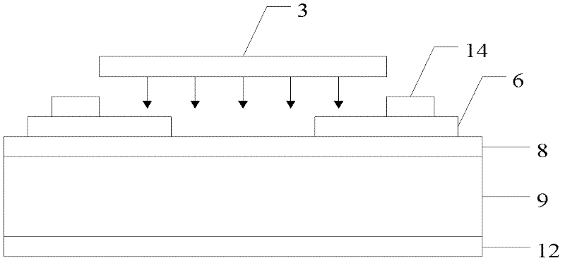
[0028] Step 1, epitaxial n-type epitaxial layer on SiC highly doped n-type substrate sample, such as Figure 5 a.

[0029] The selected doping concentration is 1×10 18 cm -3 Highly doped n-type SiC substrate sample 7, after cleaning, epitaxially grow on the highly doped n-type SiC substrate sample with a thickness of 4um, an initial n-type epitaxial layer doped with nitrogen ions, and its doping concentration is 1×10 15 cm -3 , the epitaxy temperature is 1570°C, the pressure is 100mbar, the reaction gases are silane and propane, the flow rates are 50sccm and 150sccm respectively, the carrier gas is pure hydrogen, and the impurity source is liquid nitrogen.

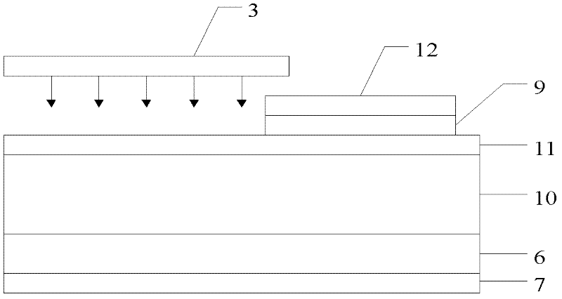
[0030] Step 2: For a nitrogen doping concentration of 1 x 10 15 cm -3 The initial n-type SiC epitaxial layer is implanted with vanadium ions, such as Figure 5 b.

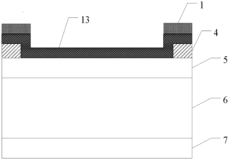
[0031] (2.1) The concentration of nitrogen doping is 1×10 15 cm -3 The initial n-type SiC epitaxial layer was implanted with vanadium ions, and the vana...

Embodiment 2

[0047] Step 1: Epitaxial n-type epitaxial layer on SiC highly doped n-type substrate sample, such as Figure 5 a.

[0048] The selected doping concentration is 5×10 18 cm -3 Highly doped n-type SiC substrate sample 7, after cleaning, epitaxially grow on the highly doped n-type SiC substrate sample with a thickness of 3um, an initial n-type epitaxial layer doped with nitrogen ions, and its doping concentration is 5×10 15 cm -3 , the epitaxy temperature is 1570°C, the pressure is 100mbar, the reaction gases are silane and propane, the flow rates are 50sccm and 150sccm respectively, the carrier gas is pure hydrogen, and the impurity source is liquid nitrogen.

[0049] Step 2: The concentration of nitrogen doping is 5×10 15 cm -3 The initial n-type SiC epitaxial layer is implanted with vanadium ions, such as Figure 5 b.

[0050] (2.1) The concentration of nitrogen doping is 5×10 15 cm -3 The initial n-type SiC epitaxial layer was implanted with vanadium ions, and the van...

Embodiment 3

[0066] Step A: Epitaxial n-type epitaxial layer on SiC highly doped n-type substrate sample, such as Figure 5 a.

[0067] The selected doping concentration is 7×10 18 cm -3 Highly doped n-type SiC substrate sample 7, after cleaning, epitaxially grow on the highly doped n-type SiC substrate sample with a thickness of 5um, an initial n-type epitaxial layer doped with nitrogen ions, and its doping concentration is 2×10 15 cm -3 , the epitaxy temperature is 1570°C, the pressure is 100mbar, the reaction gases are silane and propane, the flow rates are 50sccm and 150sccm respectively, the carrier gas is pure hydrogen, and the impurity source is liquid nitrogen.

[0068] Step B: For a nitrogen doping concentration of 2 x 10 15 cm -3 The initial n-type SiC epitaxial layer is implanted with vanadium ions, such as Figure 5 b.

[0069] (B1) The concentration of nitrogen doping is 2×10 15 cm -3 The initial n-type SiC epitaxial layer was implanted with vanadium ions, and the van...


PUM

PropertyMeasurementUnit
thicknessaaaaaaaaaa

Abstract

The invention discloses a silicon carbide Schottky junction type nuclear cell with a vanadium-doped I layer and a production method of the silicon carbide Schottky junction type nuclear cell, mainly solving the problem of lowered energy conversion efficiency in the prior art. The Schottky junction type nuclear cell provided by the invention comprises an n-type ohmic contact electrode (8), an n-type SiC substrate sample (7) with a doping concentration of 1*10<18>-7*10<18>cm<-3>, an n-type SiC epitaxial layer (6), an SiO2 passivation layer (5), a Schottky metal contact layer (4), a Schottky contact electrode (3), a bonding layer (2) and a radioisotope source layer (1) from bottom to top, wherein the n-type SiC epitaxial layer (6) which has the doping concentration of 1*10<13>-5*10<14>cm<-3> is formed through injecting vanadium ions of which the energy is 2000 KeV-2500 KeV and the dosage is 5*10<13>-1*10<15>cm<-2>. The silicon carbide Schottky junction type nuclear cell with the vanadium-doped I layer has the advantages of high electron-hole pair collection ratio, high open circuit voltage and high energy conversion efficiency, and can be served as an on-chip power supply of a microsystem, a power supply of a cardiac pacemaker and an emergency power supply of a mobile phone.

Description

technical field [0001] The invention belongs to the field of microelectronics, in particular to an I-layer vanadium-doped silicon carbide Schottky junction nuclear battery, which can be used to directly convert nuclear energy emitted by isotopes into electric energy. technical background [0002] In 1953, Rappaport discovered that the beta (β-Particle) particles produced by the decay of isotopes can generate electron-hole pairs in semiconductors. This phenomenon is called β-Voltaic Effect. Shortly thereafter, Elgin-Kidde first used the β-Voltaic Effect in power supply in 1957, and successfully manufactured the first isotope micro-battery β-Voltaic Battery. Since 1989, GaN, GaP, AlGaAs, polysilicon and other materials have been used as materials for β-Voltaic batteries. With the preparation of the wide bandgap semiconductor material SiC and the advancement of process technology, since 2006, there have been reports on SiC-based isotope micro-batteries at home and abroad. [...

Claims


Application Information

Patent Timeline
Patent Type & Authority Applications(China)
IPC IPC(8): G21H1/00H01L31/115
Inventor 郭辉张克基张玉明张玉娟韩超石彦强
Owner 陕西半导体先导技术中心有限公司
Why Eureka
Try Eureka