Lamb wave immunosensor and manufacturing method thereof
An immunosensor and sensor technology, applied in the fields of instruments, scientific instruments, measuring devices, etc., can solve the problems of difficult to achieve sensor arraying, high-throughput large-sample molecular level measurement, etc., achieve easy automation, improve test accuracy, The effect of a simple measurement process
- Summary
- Abstract
- Description
- Claims
- Application Information
AI Technical Summary
Problems solved by technology
Method used
Image
Examples
Embodiment 1
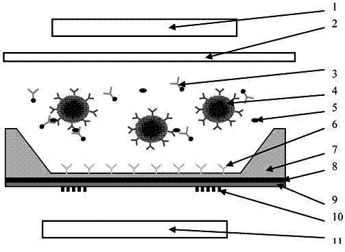
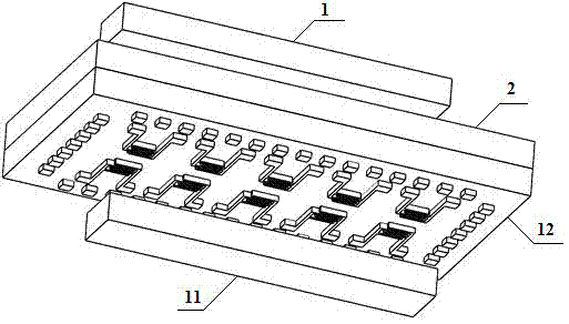
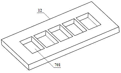
[0051] see figure 1 , figure 2 As shown, a Lamb wave immune sensor includes an upper magnet 1 and a lower magnet 11, a Lamb wave sensor 12 is arranged between the upper magnet 1 and the lower magnet 11, and a pipe pressure is glued above the Lamb wave sensor 12. Cover 2; further, combine image 3 As shown, the Lamb wave sensor 12 includes a silicon thin film structure 7 provided with a plurality of sample cells 701 , a conductive ground layer 8 is located below the silicon thin film structure 7 , and a piezoelectric material layer 9 is located below the conductive ground layer 8 , the piezoelectric material layer 9 is provided with a layer of IDT electrode layer, and further, combined with Figure 4As shown in the figure, the IDT electrode layer includes a plurality of tooth-shaping electrodes 10 and a plurality of welding point ports 13, a pair of electrode ports 14 are respectively provided on the plurality of tooth-shaping electrodes 10, and the labeled antibody 3, Immu...
Embodiment 2
[0058] see figure 1 As shown, a method for fabricating a Lamb wave device includes the following steps:
[0059] Step 1) Prepare silicon wafer: take a 3-inch, 380μm thick, double-sided oxidized P-type (100) silicon wafer with a surface thickness change of less than 3μm;
[0060] Step 2) Throwing off the photoresist: The silicon wafer is first cleaned with a mixture of acetone and alcohol, then soaked in deionized water for 5 minutes, then dried, and then the adhesive and photoresist are thrown off both sides of the silicon wafer;
[0061] Step 3) Photolithography and development: use a photolithography machine to expose the silicon wafer to generate the pattern of the template on the surface of the silicon wafer, and then put it into the developer for etching to generate the desired pattern on the photoresist layer;
[0062] Step 4) Etch the silicon dioxide: put the silicon wafer into the hydrofluoric acid solution to etch the silicon dioxide layer, so that the surface patter...
Embodiment 3
[0075] see figure 1 As shown, a method for detecting carcinoembryonic antigen, which comprises the following steps:
[0076] Step 1) Mix the analyte 5 with the immune micro-magnetic beads 4 and inject them into the sample cell 701 of the Lamb wave device 12 for co-incubation. The surface of the immune micro-magnetic beads 4 is coated with a certain carcinoembryonic antigen antibody;
[0077] Step 2) Turn on the magnetic field below the Lamb wave immunosensor, so that the immunomagnetic spheres are adsorbed to the surface of the Lamb wave device 12, and together with the capture antibody 6 on the surface of the Lamb wave device 12, form a ternary complex of "immunomagnetic sphere-analyte-antibody" thing;
[0078] Step 3) Turn on the magnetic field above the Lamb wave immunosensor, so that the immunomicromagnetic beads 4 that do not form the "immunomagnetic ball-analyte-antibody" ternary complex are adsorbed to the top of the Lamb wave device 12;
[0079] Step 4) Add washing s...
PUM
| Property | Measurement | Unit |
|---|---|---|
| thickness | aaaaa | aaaaa |
| height | aaaaa | aaaaa |
| diameter | aaaaa | aaaaa |
Abstract
Description
Claims
Application Information


