Method for carrying out bonding epitaxial wafer and silicon wafer by indium (In)

An epitaxial wafer and silicon wafer technology, which is applied in semiconductor/solid-state device manufacturing, electrical components, circuits, etc., can solve the problem of not being able to be widely used, save chemicals and equipment utilization, low melting point of indium, and reduce losses. The effect of matching defects

Inactive Publication Date: 2012-07-11
BEIJING TIMES HAODING TECH
View PDF3 Cites 8 Cited by
  • Summary
  • Abstract
  • Description
  • Claims
  • Application Information

AI Technical Summary

Problems solved by technology

Therefore, it cannot be widely used in high-brightness LED lighting

Method used


Image

  • Method for carrying out bonding epitaxial wafer and silicon wafer by indium (In)
  • Method for carrying out bonding epitaxial wafer and silicon wafer by indium (In)
  • Method for carrying out bonding epitaxial wafer and silicon wafer by indium (In)

Examples


Embodiment Construction

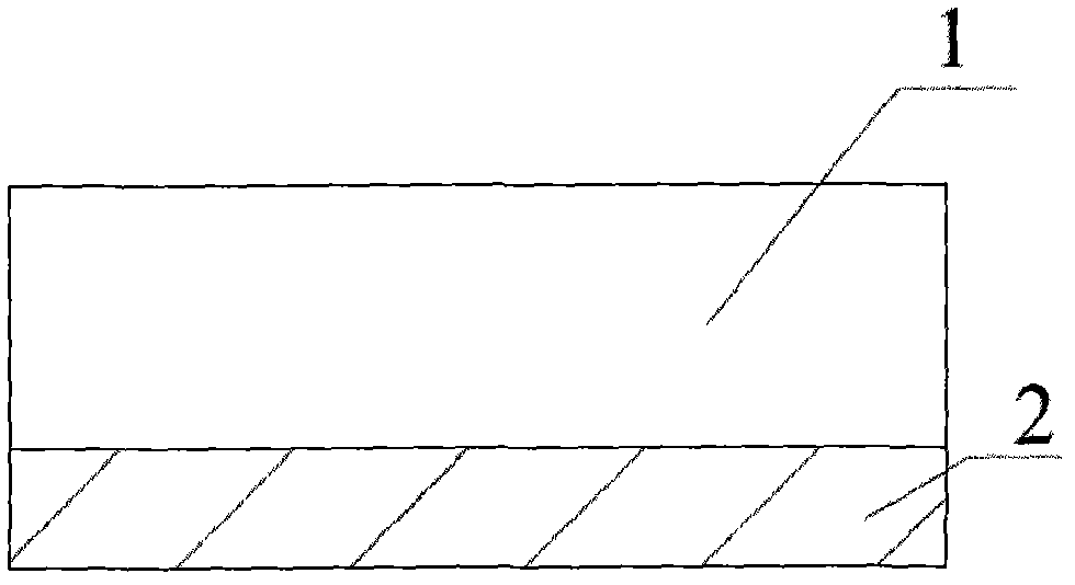
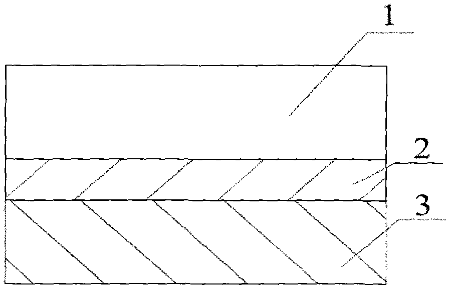
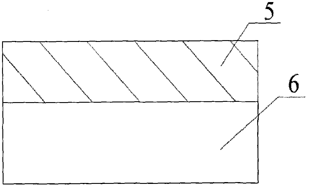
[0019] A kind of method that indium (In) carries out epitaxial wafer / silicon wafer bonding, has mirror layer (such as figure 1 The epitaxial wafer (shown in 2) (such as figure 1 As shown in 1) evaporated gold (Au) layer (such as figure 2 shown in 3), and then the mirror-polished silicon wafer (such as image 3 Shown in 6) the surface is soaked in the mixed solution (sulfuric acid, hydrogen peroxide, water) of 55 ℃ for 30 seconds, the ratio of the mixed solution can be sulfuric acid: hydrogen peroxide: water = 5: 1: 1, then rinse with deionized water, and put It is placed in a drying machine to dry, and a gold layer of a certain thickness is evaporated in an electron beam evaporation table (such as image 3 5) and indium (In) layer (such as Figure 4 shown), and then two opposite indium (In) layers are placed in the middle, put into the bonding machine (bonding) through the thermocompression bonding method, the thermocompression bonding pressure is 500KG, and the bonding te...


PUM


Abstract

The invention discloses a method for carrying out epitaxial wafer and silicon wafer bonding by indium (In). The method comprises the steps as follows: an indium (In) layer is deposited on the silicon wafer where a gold (Au) layer is evaporated, and the gold (Au) layer is evaporated on the epitaxial wafer where a reflecting mirror layer is deposited; the two wafers (the indium (In) layer in the middle) face relatively and are put into a bonding machine for bonding, so as to prepare an LED (light-emitting diode) device with the advantages of high efficiency, high brightness, low resistance and steady performance. The epitaxial wafer and silicon wafer bonding is carried out by the method, the bonding area is compact and hole-free, the bonding strength is high, and the bonding rate can reach above 98%. The bonding area of a prepared substrate slice has no pollution layer, polycrystalline layer or oxide layer, so that the performance of the prepared light-emitting diode device is greatly improved.

Description

technical field [0001] The invention belongs to the technical field of epitaxial wafer / silicon bonding in semiconductors, in particular to a method for bonding epitaxial wafers / silicon wafers with indium (In). Background technique [0002] Epitaxial wafer / silicon wafer bonding is an important new technology in the field of semiconductor optoelectronics and power electronics. It is to realize direct chemical bonding of oxidized or unoxidized epitaxial wafers and silicon wafers to form a whole without any adhesive. At present, the direct bonding methods of epitaxial wafers and silicon wafers at home and abroad usually require special surface bond enhancement treatment on the surface of epitaxial wafers and silicon wafers, which makes the bonding process complicated and the bonding results are not ideal. The bonding layer is prone to produce voids and non-bonding areas, resulting in low bonding rate and interlayers, which affect the preparation performance of the device, and t...

Claims


Application Information

Patent Timeline
Patent Type & Authority Applications(China)
IPC IPC(8): H01L21/02H01L21/20
Inventor 杨继远
Owner BEIJING TIMES HAODING TECH
Why Eureka
Try Eureka