Manufacturing method of passivated InAs/GaSb secondary category superlattice infrared detector

A technology of infrared detector and manufacturing method, applied in semiconductor device, final product manufacturing, sustainable manufacturing/processing, etc., can solve problems such as device performance degradation

Inactive Publication Date: 2012-07-11
INST OF SEMICONDUCTORS - CHINESE ACAD OF SCI
View PDF2 Cites 18 Cited by
  • Summary
  • Abstract
  • Description
  • Claims
  • Application Information

AI Technical Summary

Problems solved by technology

Its main disadvantage is that in order to obtain a dense passivation film, PECVD is usually used to deposit SiO at a substrate temperature of 300°C. 2 , exposure of superlattice materials to such high temperatures can lead to degradation of the performance of the entire device

Method used


Image

  • Manufacturing method of passivated InAs/GaSb secondary category superlattice infrared detector
  • Manufacturing method of passivated InAs/GaSb secondary category superlattice infrared detector
  • Manufacturing method of passivated InAs/GaSb secondary category superlattice infrared detector

Examples


Embodiment Construction

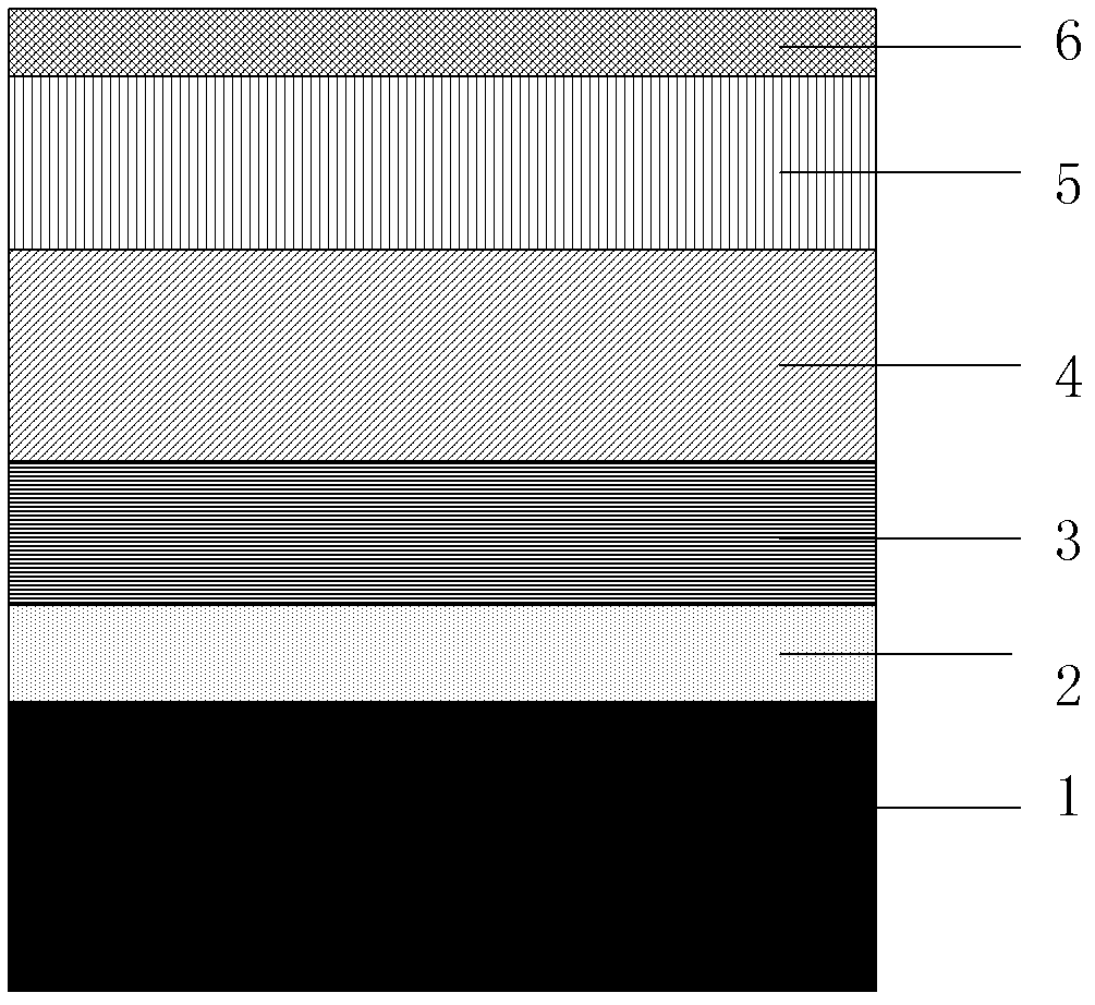
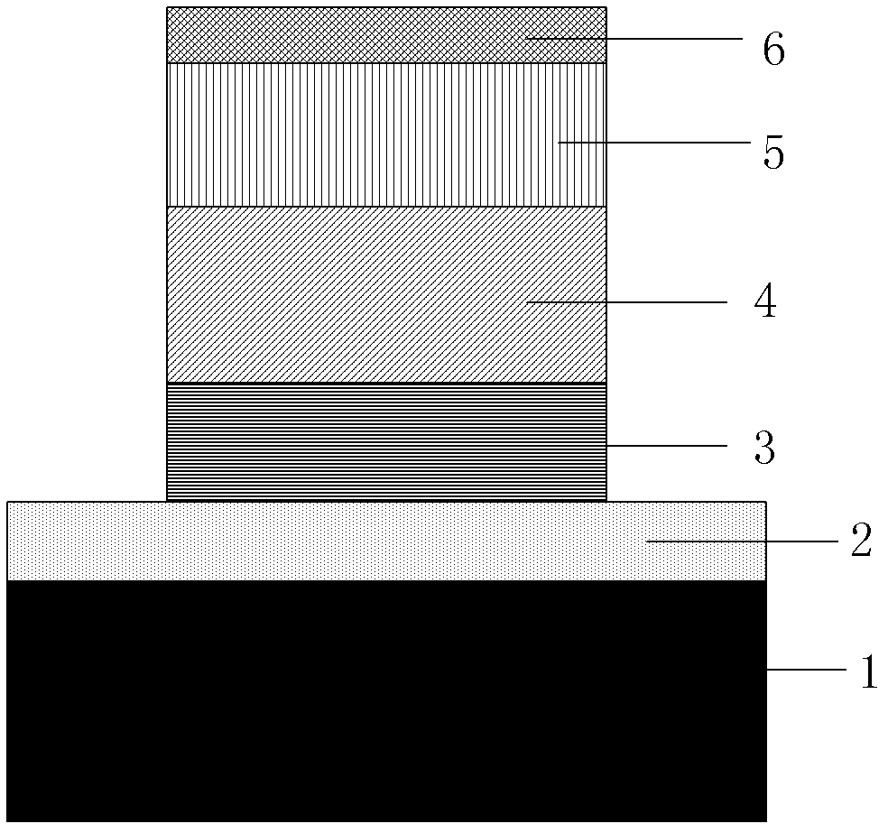
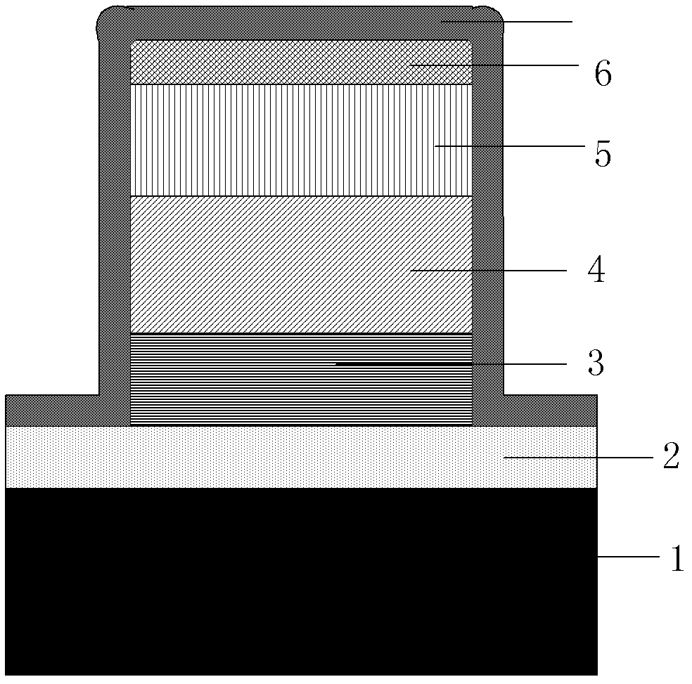
[0028] see figure 1 As shown, the present invention provides a kind of passivation InAs / GaSb class II superlattice infrared detector manufacturing method, comprises the following steps:

[0029] Step 1: Grow a P-type GaSb buffer layer 2, a P-type InAs / GaSb type II superlattice layer 3, and an intrinsic InAs / GaSb II layer sequentially on a GaSb substrate 1 by metal chemical organic vapor deposition or molecular beam epitaxy. A superlattice-like light absorption layer 4, an N-type InAs / GaSb second-type superlattice layer 5 and an N-type InAs ohmic contact layer 6 form an epitaxial wafer, and its structure is as follows figure 1 shown;

[0030] Step 2: Boil the epitaxial wafer with trichlorethylene, acetone and methanol at 50°C for 5 minutes under ultrasonic waves, then use isopropanol to dehydrate, and use N 2 Blow dry and dry in an oven;

[0031] Step 3: use the designed photolithography plate to perform the first photolithography on the epitaxial wafer, and then use citric ...


PUM


Abstract

The invention relates to a manufacturing method of a passivated InAs / GaSb secondary category superlattice infrared detector. The method comprises the following steps that: a metal organic chemical vapor deposition method or a molecular beam epitaxial method is employed to enable a buffer layer, a secondary superlattice layer, an intrinsic secondary superlattice light absorption layer, an N type secondary superlattice layer, and an N type ohmic contact layer to be successively grown on a substrate, so that an epitaxial wafer is formed; a wet etching method or a dry etching method is employed to carry out corrosion or etching on the epitaxial wafer; a spin coating machine is used to coat a resin material on the surface of the etched epitaxial wafer; exposure is carried out; medium baking and developing are carried out as well as an upper electrode and light entering window and lower electrode windows are formed on the resin material-coated epitaxial wafer; an electrode material is manufactured; photoetching is carried out on the electrode material to form upper electrodes and lower electrodes. According to the invention, a passivated infrared detector that is manufactured by the provided manufacturing method has low dark currents and ROA is increased; besides, the method has characteristics of simple manufacturing technology, strong passivation film strength and good passivation effect and the like.

Description

technical field [0001] The invention belongs to the field of semiconductor optoelectronics, in particular to a method for manufacturing a passivated InAs / GaSb type II superlattice infrared detector. Background technique [0002] In recent years, InAs / GaSb type II superlattice materials have received increasing attention, because the bottom of the conduction band of InAs in the InAs / GaSb type II superlattice is lower than the top of the valence band of InAs / GaSb, so that electrons and holes Space separation, the Auger recombination rate is greatly reduced, the carrier lifetime is longer, and in the long-wave and very long-wave bands, the InAs / GaSb type II superlattice has a more obvious inhibitory effect on the Auger recombination. Based on the above incomparable advantages, the InAs / GaSb type II superlattice detector has become the most active field of infrared detection, and is one of the ideal representatives of the third generation infrared focal plane detector. [0003]...

Claims


Application Information

Patent Timeline
Patent Type & Authority Applications(China)
IPC IPC(8): H01L31/18
CPCY02P70/50
Inventor 曹玉莲马文全张艳华
Owner INST OF SEMICONDUCTORS - CHINESE ACAD OF SCI
Why Eureka
Try Eureka