Wafer level packaging method of light emitting diode with adjustable lens focus

A light-emitting diode, wafer-level packaging technology, applied in decorative arts, micro-structure devices, manufacturing of micro-structure devices, etc. Effect

Inactive Publication Date: 2012-07-11
吕思远
View PDF5 Cites 9 Cited by
  • Summary
  • Abstract
  • Description
  • Claims
  • Application Information

AI Technical Summary

Problems solved by technology

At the same time, the encapsulation lens structure must have good airtightness, bec

Method used


Image

  • Wafer level packaging method of light emitting diode with adjustable lens focus
  • Wafer level packaging method of light emitting diode with adjustable lens focus
  • Wafer level packaging method of light emitting diode with adjustable lens focus

Examples


Embodiment 1

[0037] Example 1 A wafer-level packaging method for a light-emitting diode with adjustable lens focus, comprising the following steps:

[0038] The first step is to etch the LED lens mold micro-slot array corresponding to the light-emitting diode array and the space-controlled mold micro-slot array surrounding the light-emitting diode lens mold groove on the silicon wafer. If the groove is not connected, place an appropriate amount of thermal release agent in the micro groove of the LED lens mold; the etching method can be dry or wet etching, 4-inch silicon wafer can be used, and the thermal release agent can be calcium carbonate or titanium hydride Powder, the weighing of the powder is based on the amount of gas required for the volume of the glass micro-cavity of the required size.

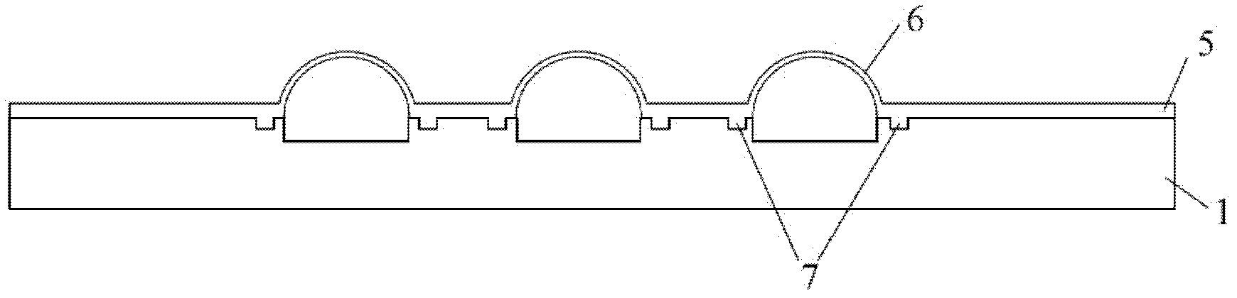
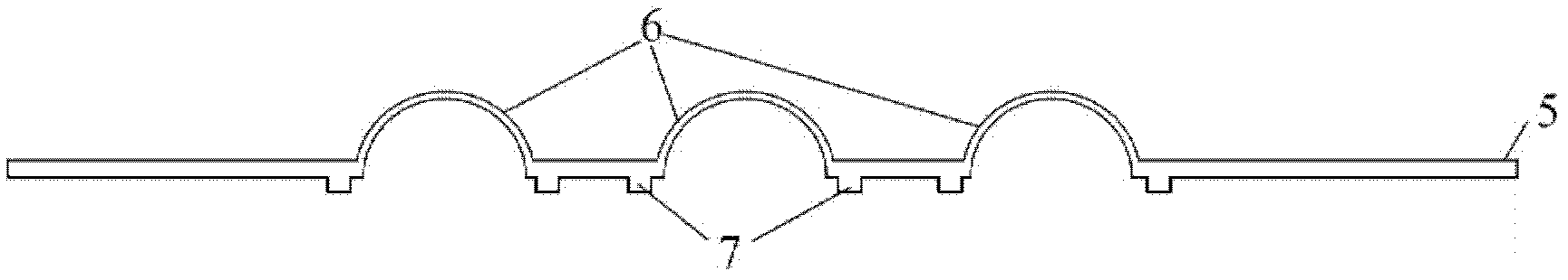
[0039] In the second step, the etched silicon wafer and the borosilicate glass wafer are anodically bonded in a vacuum to form a sealed cavity; the vacuum degree can be less than 1Pa, such as ...

Embodiment 2

[0046] Example 2 A wafer-level packaging method for light-emitting diodes with adjustable lens focus, comprising the following steps: a first step: etching a light-emitting diode lens mold micro-slot array corresponding to a light-emitting diode array and a surrounding light-emitting diode lens mold on a silicon wafer The spacing of the grooves controls the mold micro-groove array, and the LED lens mold micro-grooves are not connected to the spacing-control mold micro-grooves, and an appropriate amount of thermal release agent is placed in the light-emitting diode lens mold micro-grooves; the etching method can be dry or wet etching. For etching, a 4-inch silicon wafer can be used, and calcium carbonate can be used as a thermal release agent. The weighing of the powder is based on the gas volume required for the glass microcavity volume of the required size. For example, for a 4-inch silicon wafer, the width is 500 Micron and 50 micron deep grooves, the number of grooves is 5...

Embodiment 3

[0054] A wafer-level glass ball cavity packaging method for light-emitting diodes, comprising the following steps:

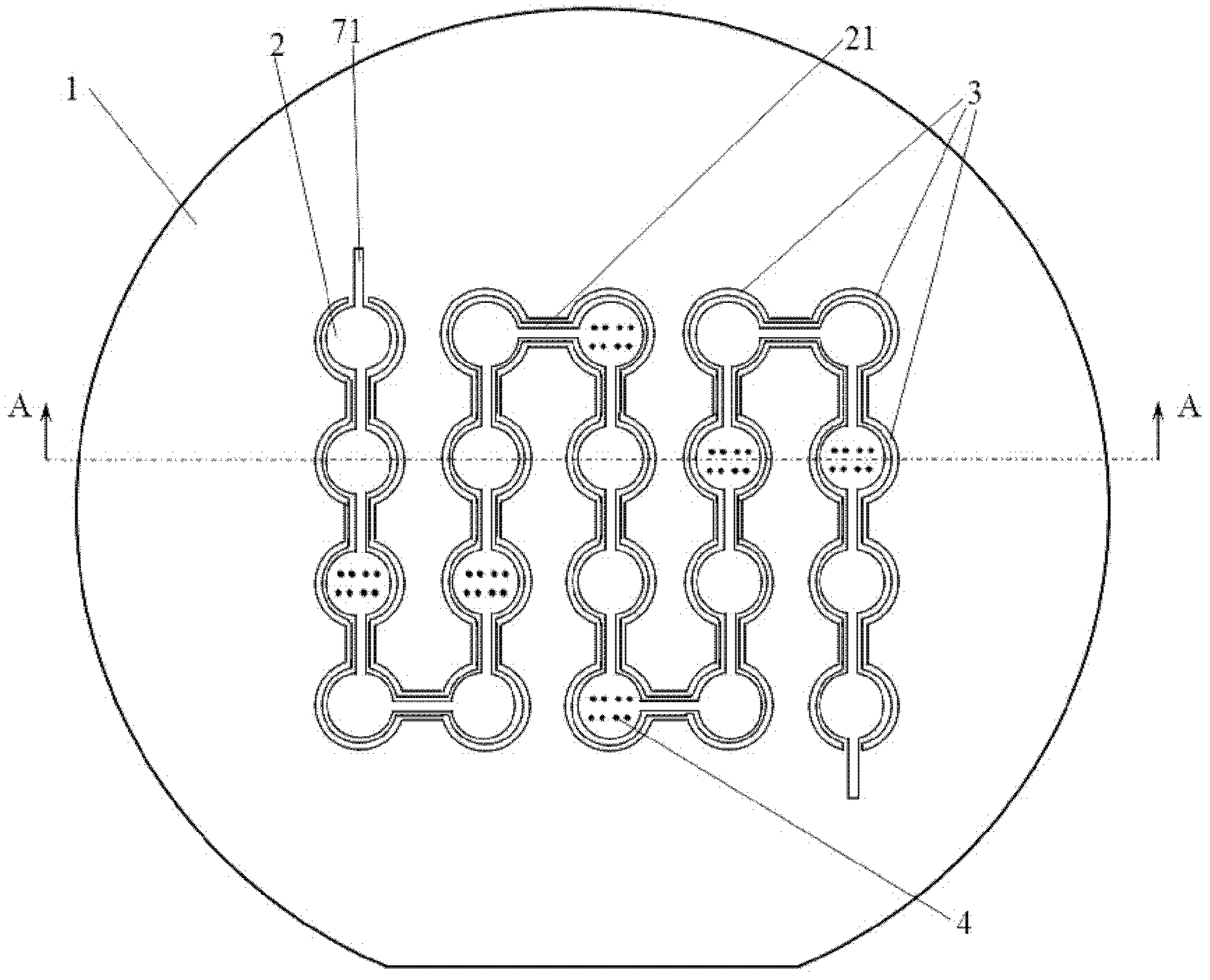
[0055] The first step is to dry-etch specific microgrooves and microchannel patterns on a Si wafer (such as a 4-inch wafer) using a Si micromachining process, and the pattern corresponding to the packaged LED array: a. Microgroove Array, the microgrooves are connected through microchannels, the microgrooves are circular, and the size ratio of the microgrooves and the microchannels is adjusted according to the preparation requirements; b. The spacing controls the mold microgrooves; evenly place an appropriate amount in the microgroove array. Thermal release agent (CaCO 3 ); In the second step, the above-mentioned Si wafer with pattern and thermal release agent is anodic-bonded with Pyrex7740 borosilicate glass wafer in air or vacuum to seal the above-mentioned micro-grooves and micro-channels to form a seal In the third step, the above-mentioned bonded wafers ar...


PUM

PropertyMeasurementUnit
Depthaaaaaaaaaa

Abstract

The invention discloses a wafer level packaging method of a light emitting diode with an adjustable lens focus. The method comprises the following steps: in a first step, etching a light emitting diode lens mould microchannel array and a spacing control mould microchannel array surrounding a light emitting diode lens mould groove on a silicon wafer, and disposing proper amount of thermal outgassing agents in a light emitting diode lens mould microchannel; in a second step, carrying out anode bonding of the silicon wafer and a borosilicate glass water in vacuum to form a sealed cavity; in a third step, carrying out heating and heat preservation on a bonding wafer in the air, forming a spherical glass micro-cavity and a spacing control projection ring, carrying out cooling and annealing, and removing silicon to obtain a light emitting diode packaging lens array; in a fourth step, pasting a light emitting diode chip on a substrate; in a fifth step, bonding a wafer level glass micro-cavity and the substrate; in a sixth step, filling up glue into a gap between a light emitting diode chip and the wafer level glass micro-cavity through a spacing control ring gap, and carrying out solidification. The method can be carried out on a wafer level, and the method has the advantages of simplicity and low cost.

Description

technical field [0001] The invention relates to a MEMS (micro-electro-mechanical system) packaging technology, in particular to a wafer-level packaging method for a light-emitting diode with adjustable lens focus. Background technique [0002] For lighting purposes, high-power white light-emitting diodes (LEDs) have been widely concerned by scientific research and enterprises. In order to generate sufficient light intensity, the working current of light-emitting diodes (LEDs) must be as large as possible, and the large working current is required for the packaging of light-emitting diodes (LEDs). The heat dissipation problem of the system has brought serious challenges. Therefore, by designing the optical packaging structure of white light-emitting diodes (LEDs) and increasing their light output rate, sufficient light intensity can be obtained under a certain current, and the lens can be used to improve the collimation of the beam, so light-emitting diodes (LEDs) There must...

Claims


Application Information

Patent Timeline
IPC IPC(8): H01L33/00B81C1/00
Inventor 吕思远
Owner 吕思远
Why Eureka
Try Eureka