Multi-wavelength semiconductor laser based on annular resonant cavity

A ring resonator and laser technology, which is applied in semiconductor laser devices, optical waveguide semiconductor structures, laser devices, etc., can solve the problems of difficult large-scale integration of devices, complex device packaging, and complex material growth, etc., to reduce the difficulty of growth , Simple and compact structure, simple preparation process

Active Publication Date: 2014-04-23
THE 13TH RES INST OF CHINA ELECTRONICS TECH GRP CORP
View PDF6 Cites 2 Cited by
  • Summary
  • Abstract
  • Description
  • Claims
  • Application Information

AI Technical Summary

Problems solved by technology

There are two types of traditional multi-wavelength lasers: one is a multi-wavelength laser that is simply combined with multiple separate single longitudinal mode lasers, or a multi-wavelength laser that is simply combined with an external wavelength selection device. One kind of device has complex packaging, large volume, high cost, and is not easy to integrate with other devices; the other is to grow an active layer structure that can generate multiple wavelength outputs on a single wafer, which is equivalent to the active layer structure of multiple single longitudinal mode lasers. Superposition of source layers, complex material growth
Moreover, traditional lasers are mostly Fabry-Perot (FP) cavity semiconductor lasers and distributed feedback (DFB) cavity semiconductor lasers, which realize resonant cavities through cleavage planes and gratings respectively, or the device is not easy due to the limitation of cleavage cavity planes. Large-scale integration, or the need to prepare gratings and high-quality secondary material growth on large-area substrates, the process is complicated and the cost is high

Method used


Image

  • Multi-wavelength semiconductor laser based on annular resonant cavity
  • Multi-wavelength semiconductor laser based on annular resonant cavity
  • Multi-wavelength semiconductor laser based on annular resonant cavity

Examples


Embodiment 1

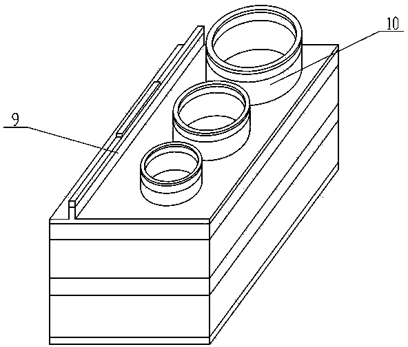
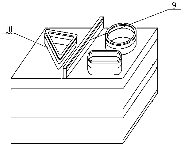
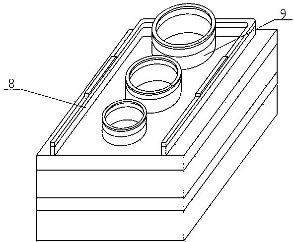
[0024] Example 1 is made of III-V compounds, and GaAs / Al is selected according to the lasing wavelength x Ga 1-x As, InP / In 1-x Ga x As y P 1-y or InP / Al x In 1-x-y Ga y As quantum well material is used as the active layer (that is, the active region) 4, where the values ​​of x and y can be designed according to the corresponding wavelength. Taking the layer structure of a laser with a wavelength of 1550nm as an example, the layer structure is grown sequentially from bottom to top on an InP substrate by using molecular beam epitaxy (MBE) or metal organic chemical vapor deposition (MOCVD) and other thin film epitaxy equipment: Doped N-type InP substrate layer 7 (i.e. lower ohmic contact layer), N-type InP buffer layer 6, 1 μm thick N-type InP lower cladding layer 5, 6 periods of AlxIn 1-x-y Ga y As multi-quantum well active layer 4, 1.6 μm thick P-type InP upper cladding layer 3, 0.3 μm thick P-type heavily doped In 0.53 Ga 0.47 As ohmic contact layer 2. Among them,...


PUM


Abstract

The invention discloses a multi-wavelength semiconductor laser based on an annular resonant cavity and belongs to the field of semiconductor lasers. The multi-wavelength semiconductor laser comprises a substrate layer, a buffer layer, a lower cladding, an active layer, an upper cladding and an ohmic contact layer which are arranged from bottom to top, wherein the laser is provided with more than one annular ridge waveguide and a coupled waveguide, each annular ridge waveguide is formed by at least the ohmic contact layer and part of the upper cladding or the whole upper cladding and can generate laser beams under forward bias, and the coupled waveguide can amplify the optical power of the laser beams under forward bias; the annular ridge waveguide and the active layer form the annular resonant cavity; the circumferences of the annular ridge waveguides are not equal; and the coupled waveguide is arranged adjacent to the annular ridge waveguides. The multi-wavelength semiconductor laser based on the annular resonant cavity has the advantages that the multi-wavelength semiconductor laser is simple and compact in structure and is easy in integration with other devices; the process is simplified, and the cost is lowered; the superposition of active layers of a plurality of single longitudinal-mode lasers is avoided, and the difficulty in the growth of materials is reduced; and the output paths of the laser beams are flexible and adjustable, and the large-scale integration of lasers is easily implemented.

Description

technical field [0001] The invention relates to a multi-wavelength semiconductor laser based on a ring resonant cavity, belonging to the field of semiconductor lasers. Background technique [0002] High-speed, high-efficiency, and large-capacity all-optical communication is the goal of the development of modern communication networks. It eliminates the conversion time of optical-electrical-optical, breaks the bottleneck of electrical transmission, and has great development potential. [0003] The light source in all-optical communication is the key device of optical communication, especially the multi-wavelength laser light source has been widely studied abroad, and its application prospect is promising. There are two types of traditional multi-wavelength lasers: one is a multi-wavelength laser that is simply combined with multiple separate single longitudinal mode lasers, or a multi-wavelength laser that is simply combined with an external wavelength selection device. One ...

Claims


Application Information

Patent Timeline
Patent Type & Authority Patents(China)
IPC IPC(8): H01S5/40H01S5/22H01S5/06
Inventor 齐利芳李献杰赵永林蔡道民尹顺政过帆
Owner THE 13TH RES INST OF CHINA ELECTRONICS TECH GRP CORP
Why Eureka
Try Eureka