Carbon-based field effect transistor and preparation method thereof

A technology of transistor and carbon base field, which is applied in the field of nanoelectronics, can solve the problems of reducing carrier mobility and device performance degradation, and achieves the effects of good reliability and repeatability, low cost and simple preparation process

Active Publication Date: 2012-07-18
INST OF MICROELECTRONICS CHINESE ACAD OF SCI
View PDF5 Cites 11 Cited by
  • Summary
  • Abstract
  • Description
  • Claims
  • Application Information

AI Technical Summary

Problems solved by technology

However, no matter which treatment method is used, an additional scattering mechanism will be introdu

Method used


Image

  • Carbon-based field effect transistor and preparation method thereof
  • Carbon-based field effect transistor and preparation method thereof
  • Carbon-based field effect transistor and preparation method thereof

Examples


Embodiment 1

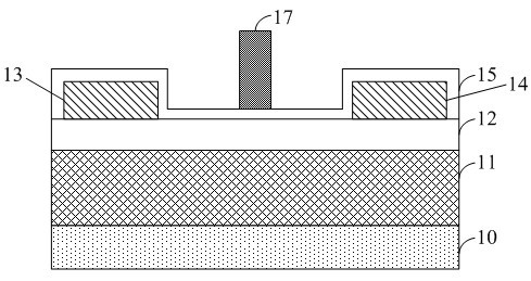
[0039] Embodiment 1: a graphene field effect transistor with metal titanium / gold as source-drain electrodes, benzocyclobutene organic dielectric layer and ALD hafnium oxide as gate composite dielectric layer, and metal nickel / gold as gate electrode.

[0040] Concrete preparation steps are as follows:

[0041] (1) On the graphene material on the 100nm silicon dioxide / bulk silicon substrate sheet, after forming the source-drain electrode shape by electron beam lithography, electron beam evaporates a layer of 10nm / 50nm thick titanium / gold (Ti / Au= 10 / 50nm) metal as the source-drain electrode, and then put the sample into acetone to peel off, remove the unnecessary metal layer, and obtain the source-drain metal electrode;

[0042] (2) Put the semiconductor substrate formed with an insulating layer, a conductive channel, a source electrode and a drain electrode into an oven filled with nitrogen, and keep the temperature of the oven at 120°C, and simultaneously coat the hexamethyldis...

Embodiment 2

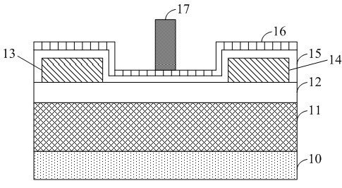
[0048] Embodiment 2: a graphene field effect transistor with metal titanium / gold as source and drain electrodes, benzocyclobutene organic dielectric layer and atomic layer deposition hafnium oxide as gate composite dielectric layer, and metal nickel / gold as gate electrode.

[0049] The specific steps are similar to those in Example 1, but the temperature of the oven in step 2 is maintained at 110°C. In step 4, the BCB is treated by rapid thermal annealing (RTA). The BCB is subjected to rapid thermal annealing at 290°C for 15 seconds to form an organic dielectric layer with a thickness of 5nm.

Embodiment 3

[0050] Embodiment 3: a graphene field effect transistor with metal titanium / gold as the source and drain electrodes, benzocyclobutene organic dielectric layer and atomic layer deposition hafnium oxide as the gate compound dielectric layer, and metal nickel / gold as the gate electrode.

[0051] The specific steps are similar to those in Example 1, but in Step 3, BCB (Cyclotene 3022-46, purchased from Dow Chemical Company, USA) and decane were diluted at a volume ratio of 1:27. After step 4, measure the thickness of the BCB organic layer to be 50nm, and the thickness of the hafnium oxide layer to be 30nm.


PUM

PropertyMeasurementUnit
Thicknessaaaaaaaaaa
Thicknessaaaaaaaaaa
Thicknessaaaaaaaaaa

Abstract

The invention relates to a carbon-based field effect transistor and a preparation method thereof, and belongs to the technical field of nanoelectronics. The carbon-based field effect transistor comprises a semiconductor substrate, an insulating layer, a conductive channel, a source electrode, a drain electrode, a gate dielectric layer and a gate electrode, wherein the insulating layer is arranged on the semiconductor substrate, and the conductive channel is arranged on the insulating layer; the conductive channel is made of a carbon-based material, and the source electrode and the drain electrode are respectively arranged at the two ends of the conductive channel; the gate dielectric layer is covered on the source electrode, the drain electrode, and the conductive channel arranged between the source electrode and the drain electrode, and the gate electrode is positioned above the gate dielectric layer; and the gate dielectric layer comprises a benzocyclobutene organic dielectric layer. According to the carbon-based field effect transistor and the preparation method thereof, the problem that a high-dielectric-constant gate dielectric film directly grows on the conductive chanel formed by a carbon-based material in the atomic layer deposition method, and the benzocyclobuten provides an atomic layer deposition nucleation center without causing a significant decrease in the carrier mobility of the carbon-based material and causing the decline in the device performance.

Description

technical field [0001] The invention relates to a field-effect transistor and a preparation method thereof, in particular to a carbon-based field-effect transistor and a preparation method thereof, and belongs to the technical field of nanoelectronics. Background technique [0002] Nanoelectronics based on carbon materials, especially those based on carbon nanotubes (Carbon Nanotube) and graphene (Graphene), are considered to have great application prospects and great potential to replace silicon-based materials. Since the successful development of carbon nanotubes in 1991 and graphene in 2004, carbon-based electronics has made great progress. Carbon-based electronics have attracted more and more attention because of their small size, high speed, low power consumption, and simple process. [0003] The performance of field effect transistors is affected by two most important factors, one is the material properties, which determine the potential of device performance; the oth...

Claims


Application Information

Patent Timeline
IPC IPC(8): H01L29/78H01L29/06H01L29/51H01L21/336H01L21/31H01L21/285
Inventor 金智麻芃郭建楠苏永波王显泰
Owner INST OF MICROELECTRONICS CHINESE ACAD OF SCI
Why Eureka
Try Eureka