Method for fabricating organic devices

A technology of organic devices and organic semiconductor layers, applied in the field of manufacturing organic devices, can solve problems such as uneven thickness of metal contacts, limiting circuit frequency, etc.

Inactive Publication Date: 2012-07-18
INTERUNIVERSITAIR MICRO ELECTRONICS CENT (IMEC VZW) +1
View PDF5 Cites 13 Cited by
  • Summary
  • Abstract
  • Description
  • Claims
  • Application Information

AI Technical Summary

Problems solved by technology

The use of shadow masking techniques for forming the metal contacts can result in non-uniform thickness of the metal contacts (ie, with "peaks" located at the edges)
When using shadow-mask techniques, the achievable channel lengths are relatively large (typically tens of micrometers) and thus limit the frequency of the corresponding circuits

Method used


Image

  • Method for fabricating organic devices
  • Method for fabricating organic devices
  • Method for fabricating organic devices

Examples


example 1

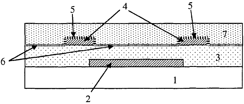
[0153] Example 1: Au Bottom Contact Transistor

[0154] Au bottom-contact organic transistors were fabricated by using a lift-off fabrication process for the formation of bottom metal contacts. In the experiments, a silicon substrate comprising a common aluminum gate and a 140 nm thick dielectric layer (silicon dioxide) was used. After cleaning the substrate provided with a patterned photoresist layer, a metallization step followed, including sputtering a 20 nm thick layer of gold and a 5 nm thick layer of aluminum. Next, perform a stripping step with acetone in an ultrasonic bath. In the transistor structure, a 20nm thick layer of gold forms the source and drain of the transistor. According to an embodiment of the invention, a 5 nm aluminum layer is used as a temporary protective layer.

[0155] After wet cleaning and UV-ozone cleaning (15 min) of the samples, a silane treatment (first surface modification layer) was performed in which PETS (phenylethyltris Chlorosilanes)...

example 2

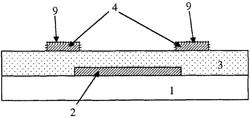
[0157] Example 2: Ag Bottom Contact Transistor

[0158] Experiments were carried out in which Ag bottom-contact transistors were fabricated according to methods of embodiments of the present invention. A metallization step is performed, consisting of providing a 15 nm thick layer of Au (used as an adhesion layer) and a 20 nm thick layer of Ag (used as a bottom contact metal, from which it can also be produced by a partial chemical reaction between silver and an electron acceptor). into a stack of "injection layers"). A 5 nm thick Al protective layer was then provided on the Ag layer. Patterning of the Au adhesion layer, Ag layer and Al protection layer was performed using a single lift-off step. After UV-ozone cleaning and silanization (formation of the first surface modification layer), within 10 minutes by mixing with diluted hydrochloric acid (1 volume concentrated hydrochloric acid + 5 volumes 2 O) to remove the Al protective layer. Next, the surface of the Ag layer is...

example 3

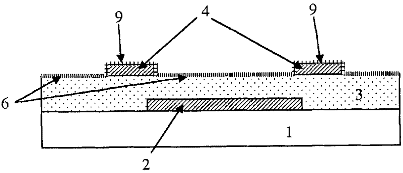
[0160] Example 3: Pd Bottom Contact Transistor

[0161] Experiments were carried out in which Pd bottom contact transistors were fabricated according to methods of embodiments of the present invention. A metallization step was performed consisting of providing a stack of a 5nm thick layer of TiW (used as an adhesion layer) and a 20nm thick layer of Pd (used as bottom contact metal). A 5 nm thick Al protective layer was then provided on the Pd layer. After UV-ozone cleaning and silanization (formation of the first surface modification layer), within 10 min by mixing with dilute sulfuric acid (1 volume of concentrated H 2 SO 4 +5 volume H 2 O) to remove the Al protective layer. For the metallization step, two different silanes were used: for one set of transistors, OTS (octadecyltrichlorosilane) was used as the first surface modification layer, and for the other set of transistors, PETS (phenylethyltrichlorosilane) was used. Chlorosilane) as the first surface modification l...


PUM


Abstract

The present invention relates to a method for fabricating an organic device, said method comprising: (i) Providing a substrate (1) having a surface comprising electrical contact structures (4) and a dielectric portion (3), (ii) Providing a first temporary protection layer (9) on some or all of said electrical contact structures (4), (iii) Providing a first surface modification layer (6) on the dielectric portion (3) and / or providing a third surface modification layer (10) on said electrical contact structures (4) not protected in step (ii), (iv) Removing the first temporary protection layer (9), (v) Providing a second surface modification layer (5) on the electrical contact structures that where protected in step (ii), and (vi) Providing said first surface modification layer (6) on the dielectric portion (3), if it was not provided in step (iii), and (vii); Providing an organic semiconductor layer (7) on top of at least part of said first surface modification layer (6) and on top of said second (5) surface modification layer and if present on top of said third surface modification layer (10), thereby obtaining said organic device or providing an organic semiconductor layer of a first type (7) on top of said second surface modification layer (5) and part of said first surface modification layer (6) and providing an organic semiconductor layer of a second type (8) on top of said third surface modification layer and another part of said first surface modification layer (6), thereby obtaining said organic device.

Description

[0001] invention technical field [0002] The present invention relates to a method of manufacturing organic devices, more particularly organic transistors, and to organic devices obtained thereby, eg organic transistors. Background of the invention [0003] Performance of organic bottom-contact transistors (where a semiconducting layer is provided on top of source / drain contacts and dielectric layers), such as pentacene transistors with gold bottom contacts and SiOx (or AlOx) dielectric layers performance can be improved by providing a silane and phosphoric acid layer on the dielectric layer and by providing a self-assembled monolayer (SAM, typically thiols) on the gold contact before depositing the pentacene layer. Such as "Molecular Self-Assembled Monolayers and Multilayers for Organic and Unconventional Inorganic Thin-Film Transistor Applications" by S.A.DiBenedetto in Advanced Materials, 2009, 21, 1407-1433 As reported in Multilayer), this approach leads to a reduction i...

Claims


Application Information

Patent Timeline
Patent Type & Authority Applications(China)
IPC IPC(8): H01L51/05H01L51/00
CPCH01L51/0017H01L51/0545H01L51/0055H01L51/0016H10K71/221H10K71/231H10K85/623H10K10/466H10K10/00
Inventor R·穆勒
Owner INTERUNIVERSITAIR MICRO ELECTRONICS CENT (IMEC VZW)
Why Eureka
Try Eureka