Manufacture method of dye sensitized solar battery based on gallium nitride (GaN) nanometer post structure

A solar cell and dye sensitization technology, applied in the field of microelectronics, can solve the problems of low electron mobility, low area, and low photoelectric conversion efficiency, and achieve the effects of stable chemical properties, high transmittance, and improved photoelectric conversion efficiency

Inactive Publication Date: 2014-09-17
XIDIAN UNIV
View PDF5 Cites 0 Cited by
  • Summary
  • Abstract
  • Description
  • Claims
  • Application Information

AI Technical Summary

Problems solved by technology

However, there are still some disadvantages in this type of battery: First, for conventional dye-sensitized solar cells, the transport path of electrons is organic materials, and the electron mobility is low during the transport process.
S

Method used


Image

  • Manufacture method of dye sensitized solar battery based on gallium nitride (GaN) nanometer post structure
  • Manufacture method of dye sensitized solar battery based on gallium nitride (GaN) nanometer post structure

Examples


Embodiment 1

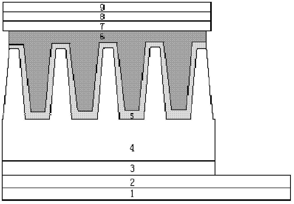
[0030] Example 1: Fabrication of a GaN nanocolumn dye-sensitized solar cell with a nanocolumn height of 600nm and a pitch of 450nm:

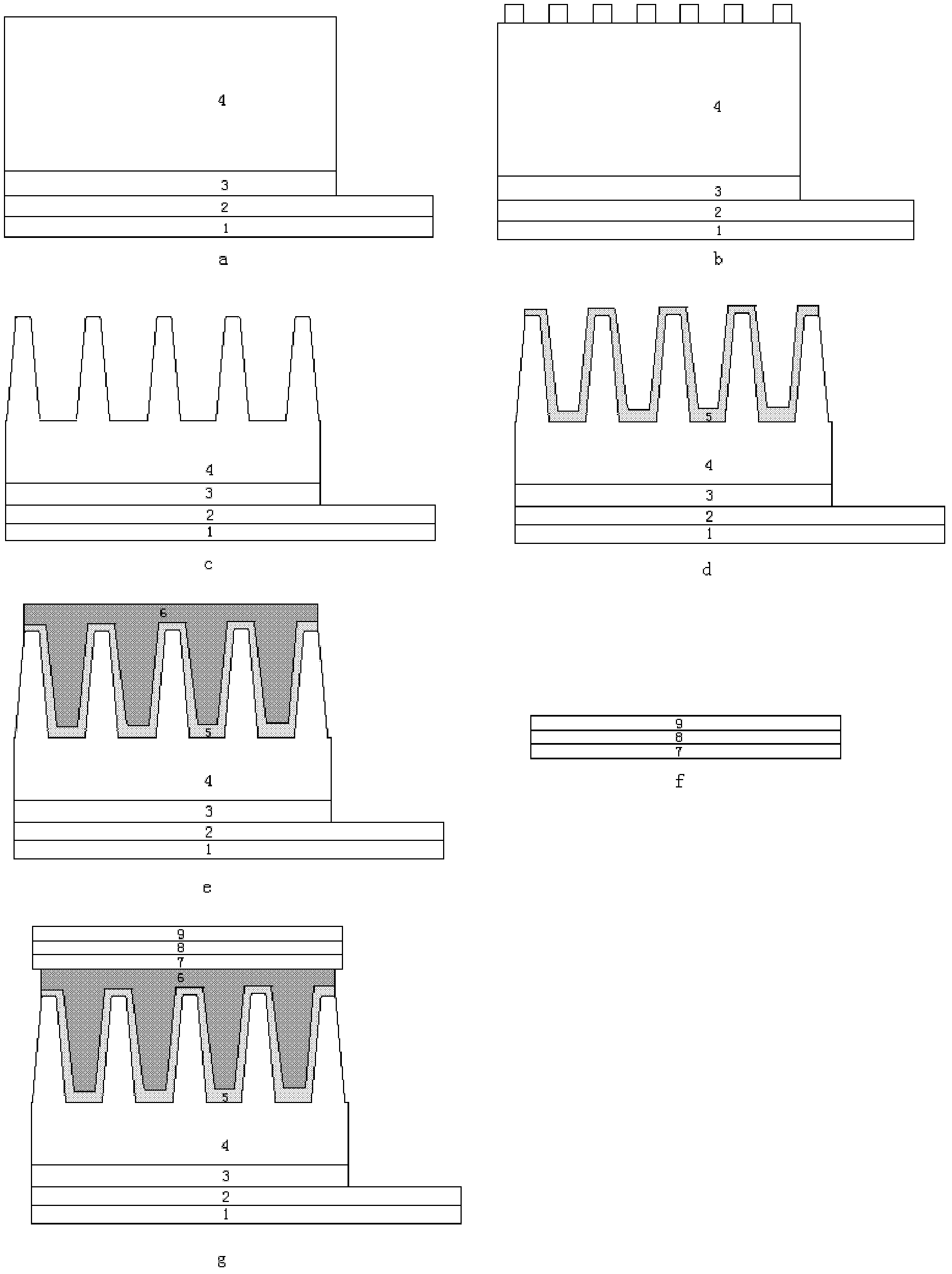
[0031] Step 1, using the ECR-PEMOCVD method to grow n-GaN layer on the indium tin oxide ITO conductive substrate, such as figure 2 a:

[0032] 1.1) Using hydrogen as the carrier gas and using high-purity nitrogen as the nitrogen source to grow a GaN buffer layer with a thickness of 60 nm on the indium tin oxide ITO, the growth process conditions are: nitrogen flow rate is 70 sccm, trimethylgallium flow rate is 0.4 sccm, The input microwave power is 550W, and the reaction temperature is 150°C;

[0033] 1.2) Keep the gas flow rate, gas composition and microwave power constant, raise the substrate temperature to 350°C, and grow an n-GaN layer on the GaN buffer layer. The n-GaN layer has a thickness of 1 μm and a carrier concentration of 1 ×10 17 cm -3 .

[0034] Step 2, put the indium tin oxide ITO conductive substrate grown with n-GaN into a...

Embodiment 2

[0049] Example 2: Fabrication of a GaN nanocolumn dye-sensitized solar cell with a nanocolumn height of 650nm and a pitch of 400nm:

[0050] Step 1, using the ECR-PEMOCVD method to grow n-GaN layer on the indium tin oxide ITO conductive substrate, such as figure 2 a.

[0051] First, using hydrogen as the carrier gas and high-purity nitrogen as the nitrogen source, the flow rate of nitrogen gas is 80 sccm, the flow rate of trimethylgallium is 0.5 sccm, the input microwave power is 600W, and the reaction temperature is 200°C. A GaN buffer layer with a thickness of 65nm is grown on tin ITO;

[0052] Then, keeping the gas flow rate, gas composition and microwave power constant, the substrate temperature was increased to 400°C, and the GaN buffer layer was grown with a thickness of 1.5 μm and a carrier concentration of 4×10 17 cm -3 n-GaN layer.

[0053] Step 2: Place the indium tin oxide ITO conductive substrate grown with n-GaN into acetone and absolute ethanol in sequence f...

Embodiment 3

[0066] Example 3: Fabrication of a GaN nanocolumn dye-sensitized solar cell with a nanocolumn height of 750nm and a pitch of 350nm:

[0067] Step A, using the ECR-PEMOCVD method to grow n-GaN layer on the indium tin oxide ITO conductive substrate, that is, first use hydrogen as the carrier gas, use high-purity nitrogen as the nitrogen source, and use the nitrogen flow rate at 75 sccm, trimethylgallium The flow rate is 0.6sccm, the input microwave power is 650W, and the reaction temperature is 185°C, a GaN buffer layer with a thickness of 70nm is grown on the indium tin oxide ITO; The bottom temperature rises to 380 °C, the thickness of the GaN buffer layer is 2 μm, and the carrier concentration is 1×10 18 cm -3 n-GaN layer, such as figure 2 a.

[0068] In step B, put the indium tin oxide ITO conductive substrate grown with n-GaN into acetone for 3 minutes for ultrasonic cleaning, then put it into absolute ethanol for 3 minutes, and finally rinse with deionized water for 15...


PUM

PropertyMeasurementUnit
Thicknessaaaaaaaaaa
Heightaaaaaaaaaa
Thicknessaaaaaaaaaa

Abstract

The invention discloses a manufacture method of a dye sensitized solar battery based on a gallium nitride (GaN) nanometer post structure and mainly solves the problem that the existing dye sensitized solar battery has low efficiency. The dye sensitized solar battery comprises a glass protection layer (1), an indium tin oxid (ITO) conducting layer (2), a GaN buffer layer (3), n-GaN nanometer posts (4), N719 dye (5), a liquid-stage electrolyte layer (6), a platinum metal layer (7), an ITO conducting layer (8) and a glass protection layer (9), wherein the n-GaN nanometer posts (4) with the height being 650nm to 750nm and the space being 350nm to 450nm are arranged between the N719 dye (5) and the GaN buffer layer (3), the ITO conducting layer (2) is positioned under the GaN buffer layer (3), the glass protection layer (1) is arranged under the ITO conducting layer (2), and the glass protection layer (1) and the ITO conducting layer (2) simultaneously form the ITO conducting glass. The manufacture method has the advantages that the battery cost is low, and the photoelectric conversion efficiency is high. The manufacture method can be used for commercial and civil power generation systems.

Description

technical field [0001] The invention belongs to the technical field of microelectronics, in particular to a dye-sensitized solar cell based on a GaN nano-column structure. Specifically, the n-GaN nanocolumn structure is formed by etching on the GaN epitaxial layer with the indium tin oxide ITO conductive glass as the substrate, and the photovoltaic characteristics are realized by covering the dye and spin-coating the electrolyte on it. . technical background [0002] The development of modern industry is increasingly dependent on energy, and how to obtain energy has gradually become the primary concern of all countries. On the one hand, because the total amount of fossil fuels is difficult to increase in a short period of time globally, and with the continuous increase of mining volume, the difficulty of obtaining them also increases. On the other hand, people pay more attention to the environment than before. Great progress has been made. Carbon dioxide and a series of su...

Claims


Application Information

Patent Timeline
IPC IPC(8): H01G9/20
CPCY02E10/542Y02P70/50
Inventor 冯倩张璐邢韬李倩郝跃
Owner XIDIAN UNIV
Why Eureka
Try Eureka