
Double-copper-electrode rectifying tube chip made of coated environment-friendly material, and coating process

A technology of environmentally friendly materials and layers of environmentally friendly materials, applied in circuits, electrical components, electrical solid devices, etc., can solve problems such as hidden environmental pollution, waste of rare resources, and no quality improvement, and achieve low-cost effects

Inactive Publication Date: 2012-08-15
HUANGSHAN GUIDING ELECTRONICS
View PDF4 Cites 3 Cited by
  • Summary
  • Abstract
  • Description
  • Claims
  • Application Information

AI Technical Summary

Problems solved by technology

The disadvantages are: due to the poor electrical and thermal conductivity of ferrous metals or Kovar alloys, the electrical and thermal conductivity of the product is affected; moreover, because it must be wrapped with lead-tin, the formula ratio of lead-tin is 95:5, a large amount of heavy metals Lead is exposed on the surface of the product, which brings major pollution risks to the environment
The disadvantage is: due to the use of precious metal silver as the coating of copper electrodes, the process cost is very high, and the production cost of products with the same rated current specification is 40% higher than that of traditional process products; Silver will be a great waste of rare resources, which is not conducive to the sustainable development of human beings; when plating silver, more cyanide is used, which is highly toxic, difficult to treat, and has serious pollution to the environment
Since the process structure was introduced from Taiwan to the mainland at the end of the last century, there has been no qualitative improvement so far.

Method used

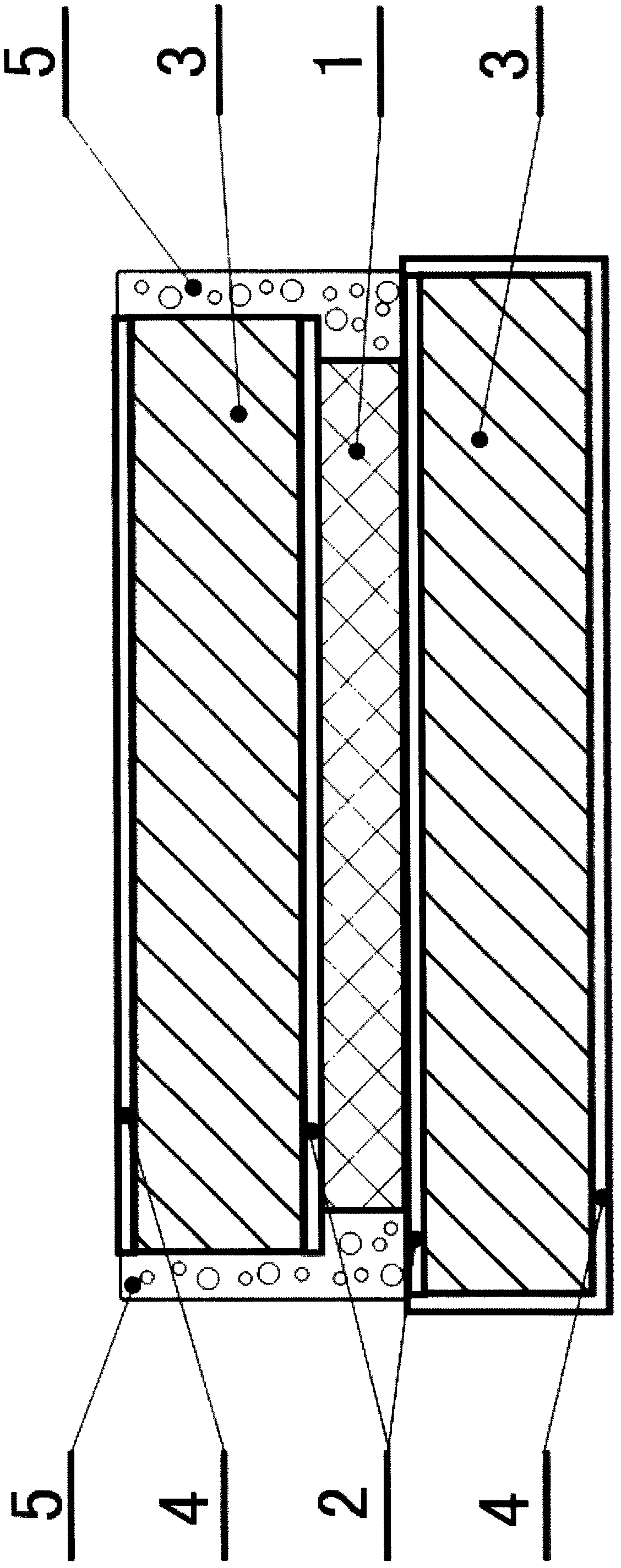
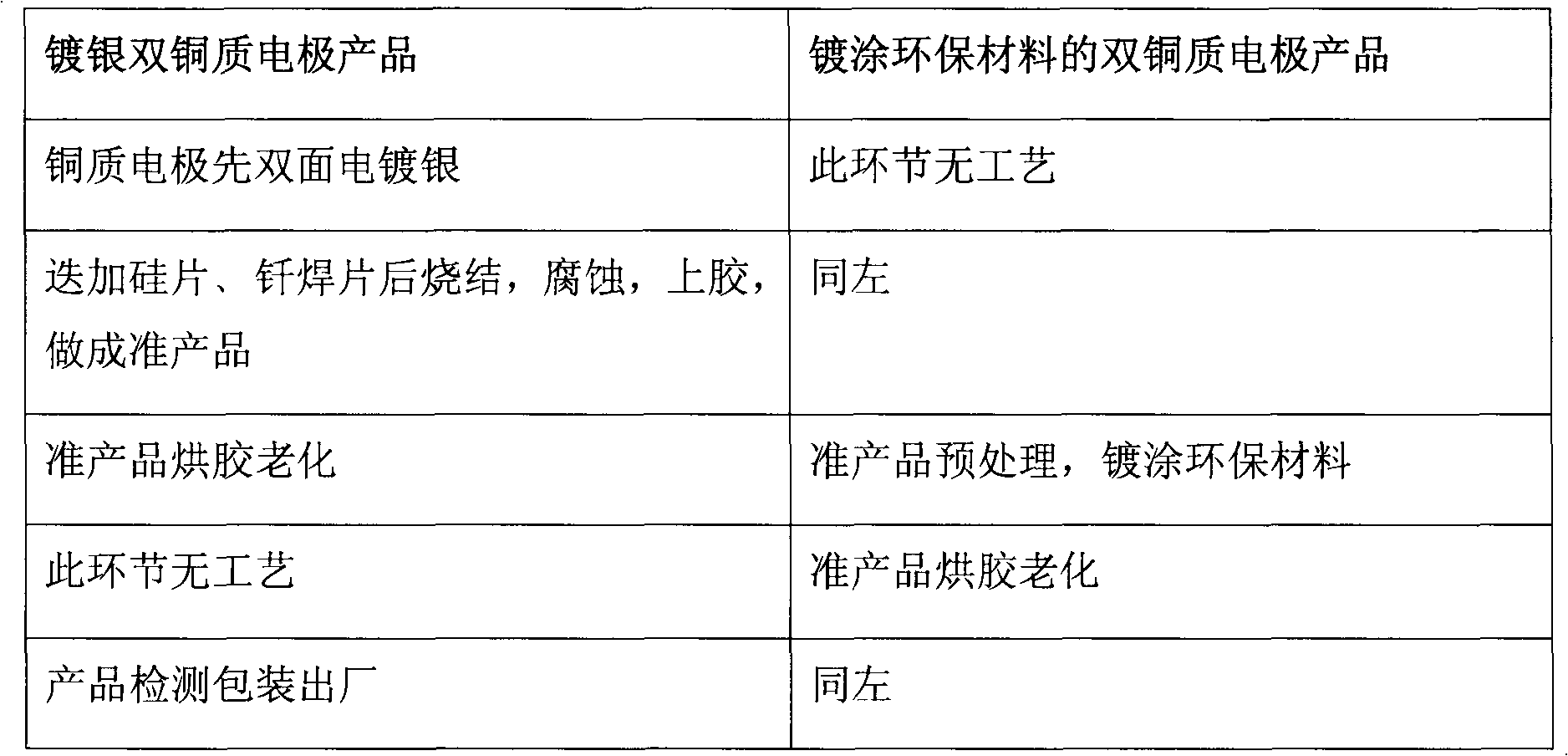
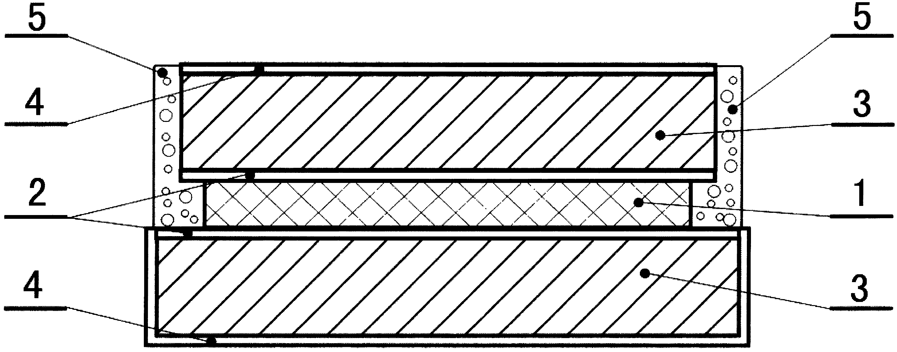

Image

  • Double-copper-electrode rectifying tube chip made of coated environment-friendly material, and coating process
  • Double-copper-electrode rectifying tube chip made of coated environment-friendly material, and coating process
  • Double-copper-electrode rectifying tube chip made of coated environment-friendly material, and coating process

Examples


Embodiment approach

[0044] 1. Several materials and accessories are purchased by outsourcing. Such as: according to the set resistivity, the set thickness, the set diffusion junction depth and concentration, the surface of the nickel-plated round silicon wafer with rectification characteristics can be 3 inches or 4 inches in diameter; the set thickness and Oxygen-free copper circle electrode with diameter; brazed circle piece with set thickness and diameter.

[0045] 2. Use a wire cutting machine to cut silicon wafers into circular, regular hexagonal, or square single silicon wafers.

[0046] 3. Put the silicon chip, brazing sheet and copper electrode in accordance with the instruction manual. figure 1 The structures shown are stacked in sequence, loaded into a sintering mold, pushed into a vacuum sintering furnace, and sintered into a quasi-product entity.

[0047] 4. Use a mixed etching solution of hydrofluoric acid, nitric acid, glacial acetic acid, and sulfuric acid to etch the vertical edg...


PUM

PropertyMeasurementUnit
Thicknessaaaaaaaaaa
Geometryaaaaaaaaaa
Diameteraaaaaaaaaa

Abstract

The invention relates to a process structure with a double-copper-electrode rectifying tube chip coated made of a coated environment-friendly material. Rectifying tube chip products about multiple contradictions, such as the quality, the cost, the resource consumption and the environment protection, can be well coordinated. The process structure has the advantages of low production cost of the conventional lead-surface process structure product and high electrothermal performance of a silver-coated double-copper-electrode product, is environment-friendly during production, does not waste noble metal and is a great technical innovation during production of the rectifying tube chip home and abroad within recent 20 years. A solid structure of the product consists of a silicon slice (1) with a rectification characteristic, a brazing layer (2), copper electrodes (3), a coated environment-friendly material layer (4) and insulative protection rubber (5).

Description

technical field [0001] The invention relates to a process structure design of a rectifier tube chip with double copper electrodes coated with environmental protection materials, which belongs to the semiconductor manufacturing technology. Background technique [0002] The rectifier chip is the basic unit product of electronic components, widely used in fields such as converters, metallurgy, automobiles, power generation, automation control and household appliances, and has a large market demand. According to industry survey data, the current annual production and sales of rectifier chips with a rated current of 3 to 100A in my country are about one billion. With the development of the economy and the popularization of automation, the market demand is still increasing at a rate of about 10% per year. [0003] Since the 1990s, the process technology for producing rectifier chips has been improved many times and has basically become mature. However, further improving product ...

Claims


Application Information

Patent Timeline
IPC IPC(8): H01L29/861H01L23/488
Inventor 胡建业程德明郑沛然胡志坚胡翰林
Owner HUANGSHAN GUIDING ELECTRONICS
Learn More