Packaging method for metal oxide semiconductor thin-film transistor

A technology for oxide semiconductors and thin film transistors, applied in semiconductor/solid-state device manufacturing, electrical components, circuits, etc., can solve problems such as destruction of semiconductors and device performance degradation, to improve stability, prevent gas molecules from interacting, and save costs. Effect

Inactive Publication Date: 2012-09-12
SHANGHAI JIAO TONG UNIV
View PDF3 Cites 14 Cited by
  • Summary
  • Abstract
  • Description
  • Claims
  • Application Information

AI Technical Summary

Problems solved by technology

At present, inorganic insulating materials (Y 2 o 3 、Al 2 o 3 , HfO 2 , SiO 2 、Si 3 N 4 etc.) Generally, radio frequency sputtering is used for deposit

Method used


Image

  • Packaging method for metal oxide semiconductor thin-film transistor
  • Packaging method for metal oxide semiconductor thin-film transistor
  • Packaging method for metal oxide semiconductor thin-film transistor

Examples


Embodiment 1

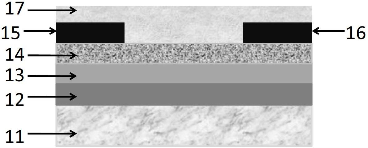
[0036] A P-type heavily doped silicon wafer is used as the insulating substrate 11, and a gate electrode 12 is prepared on the upper surface of the insulating substrate 11 by thermal evaporation using a mask with a certain pattern, and the material of the gate electrode 12 is metal; Use SiOx to prepare gate insulating layer 13 on both with thermal growth method; ZnO is prepared as metal oxide active layer 14 on gate insulating layer 13 with spin-coating process; The source electrode 15 and the drain electrode 16 are prepared on the metal oxide active layer 14; finally, polydimethylsiloxane is prepared by drop coating on the metal oxide active layer 14, the source electrode 15 and the drain electrode 16 The device protection layer 17 is annealed after film formation, and the annealing temperature does not exceed 150° C., thereby completing the packaging of the transistor.

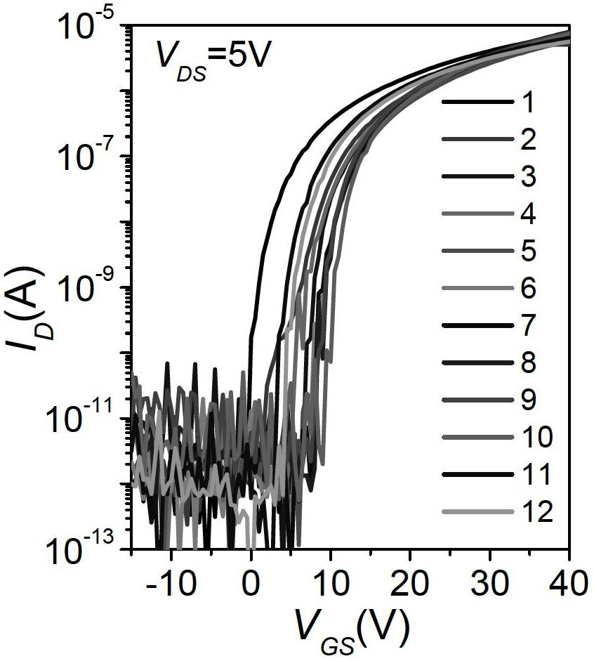
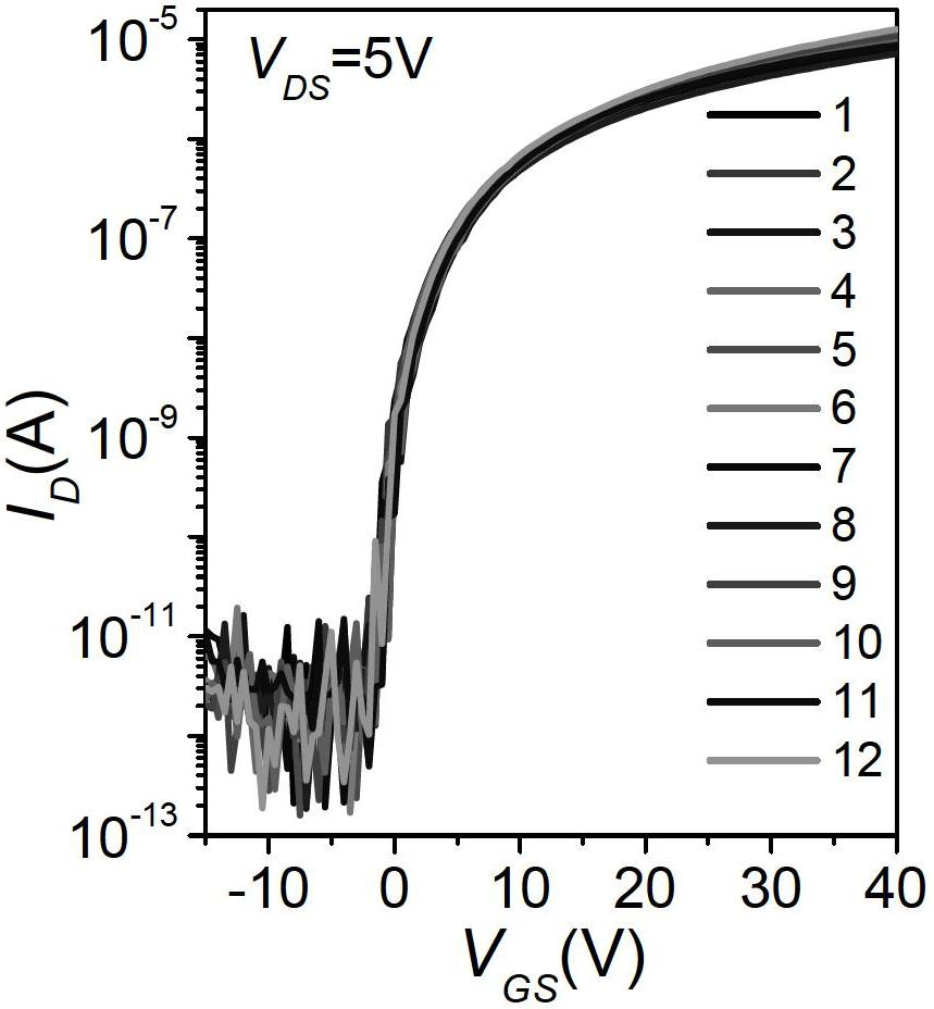
[0037] figure 2 and image 3 The performance uniformity of unpackaged metal oxide semiconductor thin f...

Embodiment 2

[0039]Adopt glass as insulating substrate 11, prepare gate electrode 12 on the upper surface of insulating substrate 11 by inkjet printing, the material of this gate electrode 12 is indium tin oxide; Gate insulating layer 13; Indium Gallium Zinc Oxide is prepared on the gate insulating layer 13 as a metal oxide active layer 14 by an inkjet printing process; metal Au is used to prepare the metal oxide active layer 14 by sputtering source electrode 15 and drain electrode 16; finally, polyvinylpyrrolidone is used to prepare the device protective layer 17 on the metal oxide active layer 14, source electrode 15 and drain electrode 16 by spin coating, annealing after film formation, and annealing The temperature does not exceed 150° C., thereby completing the packaging of the transistor.

Embodiment 3

[0041] Adopt plastic film as insulating substrate 11, prepare gate electrode 12 on the upper surface of insulating substrate 11 by photolithography, the material of this gate electrode 12 is poly 3,4-ethylenedioxythiophene / polystyrenesulfonic acid Salt; use metal oxide to prepare gate insulating layer 13 on both of them by spin coating; prepare indium gallium oxide as metal oxide active layer 14 on gate insulating layer 13 by sputtering process; use metal Ag Prepare the source electrode 15 and the drain electrode 16 on the metal oxide active layer 14 by photolithography; finally use polyvinyl alcohol to pass the pulling method on the metal oxide active layer 14, the source electrode 15 and the drain electrode 16 Method The device protective layer 17 is prepared, and annealing is performed after film formation, and the annealing temperature does not exceed 150° C., thereby completing the encapsulation of the transistor.


PUM


Abstract

The invention relates to a packaging method for a metal oxide semiconductor thin-film transistor. The thin-film transistor is packaged through a solution process. After the conventional preparation process of the metal oxide semiconductor thin-film transistor, device protection layers are prepared on the metal oxide active layer, the source electrode and the drain electrode of the thin-film transistor by adopting a spin-coating, spray-coating, drop-coating, screen-printing or puling method, and annealing is conducted after films are formed. The packaging method for the metal oxide semiconductor thin-film transistor has the advantages that the metal oxide active layer is not damaged, the stability of the device is improved, the electrical properties of the device are not damaged, at the same time the packaging cost is saved and the method is suitable for packaging the metal oxide semiconductor thin-film transistor prepared on a flexible substrate.

Description

technical field [0001] The invention relates to a manufacturing method of an electronic device, in particular to a packaging method for a metal oxide semiconductor thin film transistor, and belongs to the technical field of organic electronics. Background technique [0002] Metal oxide is a new type of wide bandgap compound semiconductor material, which has the characteristics of high electron mobility, high transmittance in the visible light range, and can be realized by a variety of processes. Thin-film transistors (TFTs) based on such semiconductor materials have been a research hotspot in recent years due to their potential applications in next-generation flat-panel display technologies, including active liquid crystal displays, active matrix organic light-emitting diode displays, and electronic paper. For unpackaged thin-film transistors with a bottom-gate structure, the active layer is exposed to the environment, so the transistor will be affected by the environment du...

Claims


Application Information

Patent Timeline
IPC IPC(8): H01L21/336
Inventor 郭小军徐小丽冯林润唐伟
Owner SHANGHAI JIAO TONG UNIV
Why Eureka
Try Eureka