JFET (Junction Field Effect Transistor) and manufacturing method thereof, and micro inverter using JFET

An N-type, channel layer technology, applied in semiconductor/solid-state device manufacturing, semiconductor devices, output power conversion devices, etc., can solve the problems of single type, slow development of SiC fully-controlled power devices, and high price, and achieve Simple structure, excellent electrical characteristics, compact size

Inactive Publication Date: 2012-09-12
CHANGAN UNIV
View PDF7 Cites 11 Cited by
  • Summary
  • Abstract
  • Description
  • Claims
  • Application Information

AI Technical Summary

Problems solved by technology

However, there are still many problems to be solved in SiC power devices. The biggest problem is that the development of SiC fully controlled power devices is relatively slow.
At present, there are only a few companies in the market that can provide a relatively single type of SiC fully-controlled power devices, and the price is too high to be widely used in civilian fields such as photovoltaics.

Method used


Image

  • JFET (Junction Field Effect Transistor) and manufacturing method thereof, and micro inverter using JFET
  • JFET (Junction Field Effect Transistor) and manufacturing method thereof, and micro inverter using JFET
  • JFET (Junction Field Effect Transistor) and manufacturing method thereof, and micro inverter using JFET

Examples


Embodiment 1

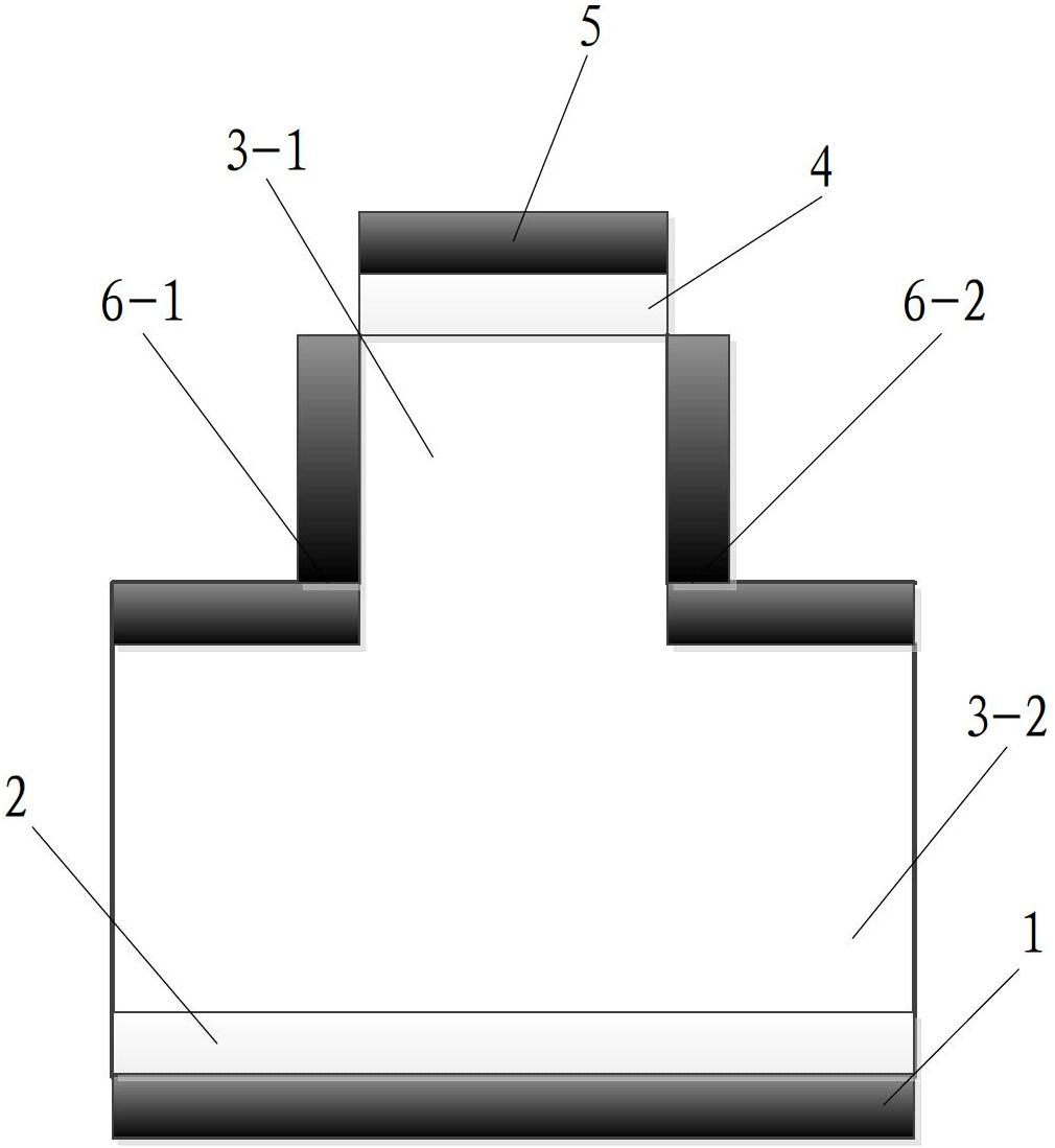
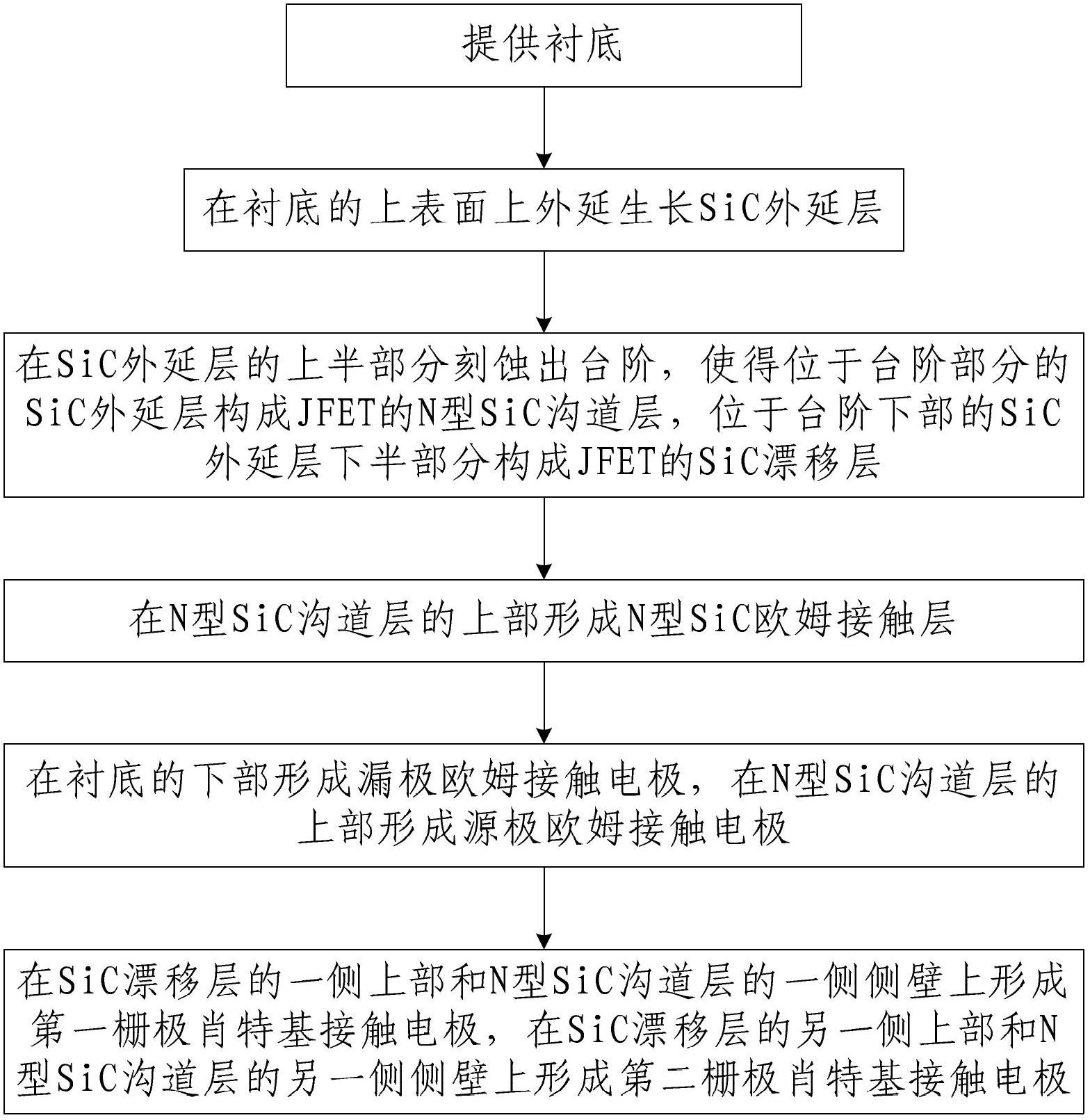
[0042] combine figure 2 , the manufacturing method of JFET described in the present invention, comprises the following steps:

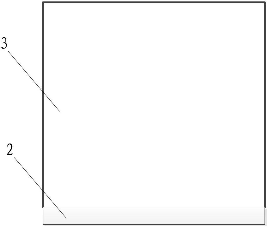
[0043] Step 1, providing a substrate 2, which is composed of an N-type SiC substrate;

[0044] Step 2. Epitaxial growth on the upper surface of the substrate 2 with a doping concentration of 5×10 by using a low pressure hot wall chemical vapor deposition method 16 cm -3 , a SiC epitaxial layer 3 with a thickness of 5 μm, the epitaxial growth temperature is 1570° C., the epitaxial growth pressure is 100 mbar, and the epitaxial growth gas is C with a volume ratio of 2:1:4. 3 h 8 、SiH 4 and H 2 The mixed gas; the structure diagram of JFET when step 2 is completed is as follows Figure 3a shown;

[0045] Step 3, using reactive ion dry etching method and using SF 6 Gas-generated plasma etches a step with a width of 0.5 μm and a thickness of 1 μm on the upper half of the SiC epitaxial layer 3, so that the SiC epitaxial layer 3 at the stepped portio...

Embodiment 2

[0051] The difference between this embodiment and embodiment 1 is that in step 2, a doping concentration of 12×10 is epitaxially grown on the upper surface of the substrate 2 by using a low pressure hot wall chemical vapor deposition method. 16 cm -3 , a SiC epitaxial layer 3 with a thickness of 10 μm; in step 3, reactive ion dry etching and SF 6 The plasma generated by the gas etches a step with a width of 0.9 μm and a thickness of 1.5 μm on the upper half of the SiC epitaxial layer 3; in step 4, ion implantation is used in the N-type SiC channel layer 3-1 The upper part is formed with a doping concentration of 3×10 18 cm -3 N-type SiC ohmic contact layer 4, and thermal annealing at a temperature of 1575° C. for 10 minutes under an Ar atmosphere; in step five, on the lower part of the substrate 2 and the upper part of the N-type SiC channel layer 3-1 Metal Ni and Pt were sequentially evaporated by electron beam, and the N 2 Thermal annealing at a temperature of 975°C for ...

Embodiment 3

[0054] The difference between this embodiment and Embodiment 1 is that in step 2, a low-pressure hot-wall chemical vapor deposition method is used to epitaxially grow on the upper surface of the substrate 2 with a doping concentration of 20×10 16 cm -3 , a SiC epitaxial layer 3 with a thickness of 15 μm; in step 3, reactive ion dry etching and SF 6 Gas-generated plasma etches a step with a width of 1.25 μm and a thickness of 2 μm on the upper half of the SiC epitaxial layer 3; in step 4, an ion implantation method is used in the upper half of the N-type SiC channel layer 3-1 The upper part is formed with a doping concentration of 5×10 18 cm -3 N-type SiC ohmic contact layer 4, and thermal annealing at a temperature of 1600° C. for 10 minutes in an Ar atmosphere; in step five, on the lower part of the substrate 2 and the upper part of the N-type SiC channel layer 3-1 Metal Ni and Pt were sequentially evaporated by electron beam, and the N 2 Thermal annealing at a temperatur...


PUM


Abstract

The invention discloses a JFET (Junction Field Effect Transistor) and a manufacturing method thereof, and a micro inverter using the JFET. The JFET comprises a drain ohmic contact electrode, a substrate, a SiC drift layer, an N-type SiC channel layer, an N-type SiC ohmic contact layer and two gate Schottky contact electrodes. The manufacturing method comprises the following steps of providing the substrate; forming a SiC epitaxial layer; forming the N-type SiC channel layer and the SiC drift layer; forming the N-type SiC ohmic contact layer; forming drain and source ohmic contact electrodes; and forming the two gate Schottky contact electrodes. The micro inverter comprises capacitors C1, C2 and C3, an inductor L1, a JFET1, a JFET2 and a JFET3, and silicon carbide Schottky diodes D1, D2, D3 and D4. According to the JFET, the manufacturing method thereof, and the micro inverter, the realization is convenient, the cost is low, the working frequency and the working reliability of the micro inverter are improved, the loss and the price of electric energy are reduced, and the practicality is high.

Description

technical field [0001] The invention relates to the technical field of semiconductor devices and semiconductor technology, in particular to a JFET, a manufacturing method thereof and a micro-inverter using the JFET. Background technique [0002] Photovoltaic power generation technology is considered to be the most promising new energy technology in the world today. Inverters are key devices in solar photovoltaic systems. At present, the grid-connected inverter products on the market are mainly centralized inverters, which connect photovoltaic cells in series and parallel to achieve a high-voltage DC, and then convert it to AC through the inverter. Due to the unbalanced performance of the battery panel, local shadows or dirt, different aging degrees, etc., it is easy to cause system mismatch and cause a decrease in output efficiency, which in turn leads to a significant decrease in overall output power. This is a difficult problem for centralized inverters. [0003] A micr...

Claims


Application Information

Patent Timeline
Patent Type & Authority Applications(China)
IPC IPC(8): H01L29/808H01L29/10H01L29/423H01L21/337H02M7/537
Inventor 张林李演明邱彦章
Owner CHANGAN UNIV
Why Eureka
Try Eureka