

Preparation method of copper indium selenium sulfide thin film for solar cell
A technology of copper indium selenium sulfur and solar cells, which is applied in the manufacture of circuits, electrical components, and final products, can solve problems such as toxicity, explosive instability, etc., achieve low cost, realize industrialized mass production, and promote rapid industrialization The effect of development
- Summary
- Abstract
- Description
- Claims
- Application Information
AI Technical Summary
Problems solved by technology
Method used
Image

Examples
Embodiment 1
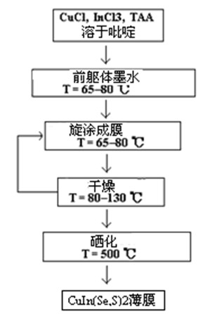
[0045] First, 0.1188 g CuCl, 0.2639 g InCl 3 4H 2 O, 0.2028 g thioacetamide was successively dissolved in 6 ml pyridine solvent, and stirred thoroughly until a pale yellow emulsion. Heating to 65 °C and stirring for 10 min, the system changed from emulsion to yellow transparent solution, and finally to blue-black precursor ink;
[0046] Secondly, the obtained blue-black ink was spin-coated, and the precursor film was coated on the soda-lime glass Mo substrate at a speed of 1500 r / min, dried in a vacuum oven for 1 min, and spin-coated once. Thin films of thin films around 500 nm are produced;
[0047] Finally, a certain thickness of the precursor film sample and selenium particles were placed in a self-made graphite box, the selenium particles were placed in the groove under the film sample, and the selenium vapor could fill the entire graphite box through the slot hole, and the graphite box was placed in a tubular in the annealing furnace, at N 2 The annealing treatment is...
Embodiment 2
[0050] First, 0.1426 g CuCl, 0.2639 g, InCl 3 4H 2 O, 0.3380 g thioacetamide was successively dissolved in 6 ml pyridine solvent, and stirred thoroughly until a pale yellow emulsion. Heating to 70 °C and stirring for 10 min, the system changed from emulsion to yellow transparent solution, and finally to blue-black precursor ink;
[0051] Secondly, the obtained blue-black ink was spin-coated, and the precursor film was coated on the soda-lime glass Mo substrate at a speed of 1500 r / min, dried in a vacuum drying oven for 1 min, and then spin-coated twice , can prepare films with different thicknesses of 1400-1500 nm;
[0052] Finally, a certain thickness of the precursor film sample and selenium particles were placed in a self-made graphite box, the selenium particles were placed in the groove under the film sample, and the selenium vapor could fill the entire graphite box through the slot hole, and the graphite box was placed in a tubular in the annealing furnace, at N 2 Th...
Embodiment 3
[0054] a) Precursor ink preparation: Dissolve Cu, In, and S-containing compounds in an appropriate amount of pyridine solvent at a Cu:In:S molar ratio of 4.8:3:12, heat to 80 °C, and stir for 15 min. Get blue-black precursor ink;
[0055] b) Precursor thin film preparation: apply the ink described in step a to coat the precursor thin film on the soda-lime glass Mo substrate by spin-coating, and then spin-coat repeatedly once to prepare a thin film with a thickness of 1000 nm;
[0056] c) Drying: Dry the precursor film prepared in step b at 80 °C for 5 min, and then spin-coat at 1500 r / min for drying;
[0057] d) Annealing treatment: performing selenization annealing treatment on the dried precursor thin film in step c to form a copper indium selenide sulfur thin film. The Cu-containing compound in step a) is CuCl, and the In-containing compound is InCl 3 4H 2 O; the sulfur-containing compound is thioacetamide, and dissolving into an appropriate amount of pyridine means reac...
PUM
| Property | Measurement | Unit |
|---|---|---|
| thickness | aaaaa | aaaaa |
| boiling point | aaaaa | aaaaa |
| band gap | aaaaa | aaaaa |
Abstract
Description
Claims
Application Information