All-oxide ferroelectric photodiode and preparation method thereof

A technology of photodiodes and oxides, used in circuits, electrical components, ion implantation plating, etc.

Active Publication Date: 2020-01-14
UNIV OF JINAN
View PDF1 Cites 3 Cited by
  • Summary
  • Abstract
  • Description
  • Claims
  • Application Information

AI Technical Summary

Problems solved by technology

But even if there is a good ferroelectric semiconductor material, there is still a long way to...

Method used


Image

  • All-oxide ferroelectric photodiode and preparation method thereof
  • All-oxide ferroelectric photodiode and preparation method thereof
  • All-oxide ferroelectric photodiode and preparation method thereof

Examples


Embodiment 1

[0055] 1. Base cleaning

[0056] STO was used as the substrate, and each process was ultrasonically cleaned in acetone, absolute ethanol, and deionized water for 15 minutes, and then dried with high-purity nitrogen.

[0057] 2. Preparation of LSMO layer

[0058] 1) Configuration of precursor solution

[0059] Mix according to the volume ratio of glacial acetic acid: deionized water = 1:1, and add equal mass of polyethyleneimine (PEI) and ethylenediaminetetraacetic acid (EDTA) to the above mixed solvent, according to the molar ratio La: Sr: Mn=7:3:10 weighing (CH 3 COOH) 3 La, (CH 3 COOH) 2 Sr and (CH 3 COOH) 2 Mn was added to a mixed solvent containing PEI and EDTA, and mixed evenly to obtain a precursor solution. The concentration of LSMO in the precursor solution was 0.1 mol / L, and the concentrations of PEI and EDTA in the precursor solution were equal, both 0.03 g / L ml;

[0060] 2) Preparation of monolayer film

[0061] (100) SrTiO 3 The substrate is placed in a ...

Embodiment 2

[0079] Prepare the device according to the method of Example 1, the difference is: when preparing the LSMO layer, the O in the furnace during the heat treatment process 2 The flow rate is 0.5 L / min.

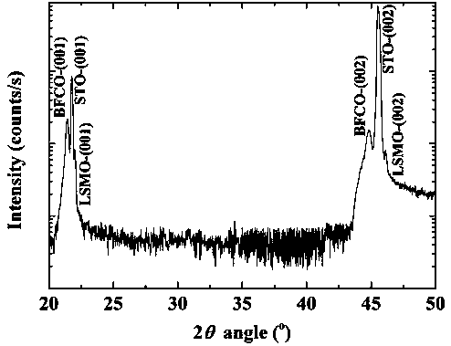
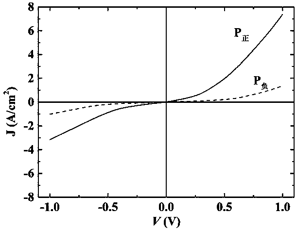
[0080] The materials of the LSMO layer and the BFCO layer in the obtained device have better epitaxial growth, and the crystallinity of the ITO layer is still good. For the device under light (AM1.5G, 100 mW cm -2 ) and the current and voltage performance under dark conditions were tested, and the test method was the same as in Example 1. The on-off ratio under dark conditions and positive and negative remanent polarization is 4.8:1; under positive and negative remanent polarization, the maximum open circuit voltage of the device under light conditions is 52 mV, and the short circuit current is 630 μA / cm 2 .

Embodiment 3

[0082] Prepare the device according to the method of Example 1, the difference is: when preparing the BFCO layer, the temperature in the furnace during the heat treatment N 2 The flow rate is 1 L / min.

[0083] The materials of the LSMO layer and the BFCO layer in the obtained device have better epitaxial growth, and the crystallinity of the ITO layer is still good. For the device under light (AM1.5G, 100 mW cm -2 ) and the current and voltage performance under dark conditions were tested, and the test method was the same as in Example 1. The on-off ratio under dark conditions and positive and negative remanent polarization is 4.6:1; under positive and negative remanent polarization, the maximum open circuit voltage of the device under light conditions is 43 mV, and the short circuit current is 520 μA / cm 2 .


PUM

PropertyMeasurementUnit
Film thicknessaaaaaaaaaa
Thicknessaaaaaaaaaa
Roughnessaaaaaaaaaa

Abstract

The invention discloses an all-oxide ferroelectric photodiode and a preparation method thereof, and the all-oxide ferroelectric photodiode comprises a substrate, the substrate is covered with an LSMOlayer, the LSMO layer is covered with a BFCO layer, and the BFCO layer is covered with an ITO layer. The LSMO layer is a La0. 7Sr0. 3MnO3 thin film which grows in an epitaxial mode, and the BFCO layeris a BiFe0. 7Co0. 3O3-delta thin film which grows in an epitaxial mode. Separation and efficient collection of photo-induced electron hole pairs in a device are promoted by utilizing ferroelectric polarization and the coupling effect of Schottky junction region barriers between electrodes, the modulation of photocurrent response and ferroelectric polarization on diode current is enhanced, the advantages of ferroelectricity and semiconductivity are both achieved, the large photocurrent response is achieved, and the polarization adjustability is good.

Description

technical field [0001] The invention relates to an all-oxide ferroelectric photodiode and a preparation method thereof, belonging to the technical field of lead-free ferroelectric photodiode devices. Background technique [0002] In two opposite ferroelectric polarization states, the ferroelectric diode exhibits a high conductance state and a low conductance state, and bipolar switching between the two states can be realized, which in turn can realize non-destructive readout of binary information. The device features ultra-fast operation (1-2 ps, depending on polarization switching time) with an ultra-high on-off ratio (up to 1:3000). However, most ferroelectrics are wide bandgap semiconductors, which limit the maximum diode current to ≈20mA cm -2 On the order of magnitude, it is difficult to stably detect the storage logic state using the sense amplifier in the existing circuit, so people have to develop semiconducting ferroelectric materials with excellent ferroelectricit...

Claims


Application Information

Patent Timeline
IPC IPC(8): H01L31/18H01L31/032C23C14/58C23C14/28C23C14/08
CPCC23C14/08C23C14/28C23C14/5806H01L31/0321H01L31/18
Inventor 杨锋刘芬林延凌季凤岐岳炳臣
Owner UNIV OF JINAN
Why Eureka
Try Eureka