Up-and-down-conversion luminescent high-transmittance amorphous fluoride film and preparation method thereof
A fluoride, high-transparency technology, applied in chemical instruments and methods, photovoltaic power generation, luminescent materials, etc., can solve problems such as low transmittance, and achieve the effects of high transmittance, uniform film surface, and simple composition.
- Summary
- Abstract
- Description
- Claims
- Application Information
AI Technical Summary
Problems solved by technology
Method used
Image
Examples
Embodiment 1
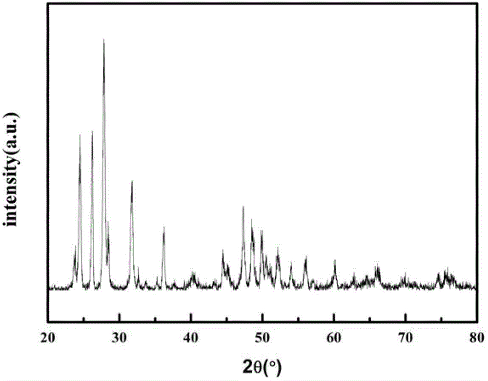
[0032] (1) In YbF 3 ErF is added to the powder 3 Powder, of which ErF 3 The powder mole fraction is 5%, then ball-milled and mixed, dried and then pressed into tablets, and then calcined at 600°C for 8 hours by carbon coating to make a ceramic target. XRD pattern of its ceramic target (see figure 1 ) Basically in line with YbF 3 PDF 34-0102 Diffraction standard spectrum.
[0033] (2) YbF prepared by the above method 3 :Er ceramic target, using electron beam deposition method: use silicon wafer as substrate, under vacuum conditions, substrate temperature is 500℃, target spacing is 32cm, deposition beam current is 4, deposition time is 15min, and YbF is obtained 3 film.
Embodiment 2
[0035] (1) In YbF 3 ErF is added to the powder 3 Powder, of which ErF 3 The molar fraction of the powder is 5%, then ball-milled and mixed, dried and then pressed into tablets, and calcined at 650°C for 8 hours by carbon coating method to make a ceramic target.
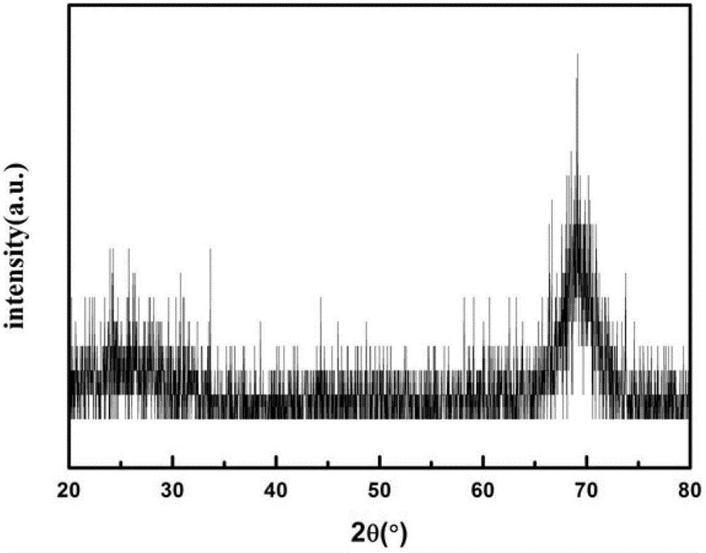
[0036] (2) YbF prepared by the above method 3 :Er ceramic target, using electron beam deposition method: using silicon wafer as substrate, under vacuum conditions, substrate temperature is 500℃, target spacing is 32cm, deposition beam current is 3, deposition time is 60min, and YbF is obtained 3 Film, see the XRD pattern figure 2 .
Embodiment 3
[0038] (1) In YbF 3 ErF is added to the powder 3 Powder, of which ErF 3 The molar fraction of the powder is 10%, then ball-milled and mixed, dried and then pressed into tablets, and calcined at 750°C for 8 hours by carbon coating, and then fired into a ceramic target. See its XRD pattern image 3 .
[0039] (2) YbF prepared by the above method 3 :Er ceramic target, using electron beam deposition method: use silicon wafer as substrate, under vacuum condition, substrate temperature is 500℃, target spacing is 32cm, deposition beam current is 5, deposition time is 60min, and YbF is obtained 3 Film, see the XRD pattern Figure 4 . Use FLS920 fluorescence spectrometer to measure the room temperature emission spectrum under 378nm excitation conditions. For the emission spectrum, see Figure 5 ;Luminescence spectrum under 980nm excitation see Image 6 .
PUM
| Property | Measurement | Unit |
|---|---|---|
| refractive index | aaaaa | aaaaa |
Abstract
Description
Claims
Application Information


