
Method for growing high-quality gallium nitride epitaxial film on basis of gallium nitride substrate

A gallium nitride substrate and epitaxial thin film technology, applied in the semiconductor field, can solve the problems affecting the practical progress of GaN-based materials, and achieve the effects of simple and easy method, short growth period and high crystal quality

Active Publication Date: 2012-10-10
NO 55 INST CHINA ELECTRONIC SCI & TECHNOLOGYGROUP CO LTD
View PDF9 Cites 18 Cited by
  • Summary
  • Abstract
  • Description
  • Claims
  • Application Information

AI Technical Summary

Problems solved by technology

However, the high-density material defects in GaN heteroepitaxial thin films still greatly affect the practical progress of GaN-based materials in the fields of microelectronics, lasers, and ultraviolet LEDs.

Method used


Image

  • Method for growing high-quality gallium nitride epitaxial film on basis of gallium nitride substrate
  • Method for growing high-quality gallium nitride epitaxial film on basis of gallium nitride substrate
  • Method for growing high-quality gallium nitride epitaxial film on basis of gallium nitride substrate

Examples


Embodiment 1

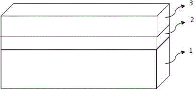
[0017] Such as figure 1 As shown, a method for growing a high-quality gallium nitride epitaxial film based on a gallium nitride substrate of the present invention is characterized in that it comprises the following steps:

[0018] 1) Select a substrate 1, which is a 0001-plane self-supporting gallium nitride substrate material;

[0019] 2) Put the substrate 1 into the metal organic chemical vapor deposition system, pass H 2 , the reaction chamber pressure is 100torr, and heated at 1050°C for 5min to clean the substrate surface and remove surface contamination;

[0020] 3) The temperature of the reaction chamber is lowered to 1000°C, and high-purity ammonia gas is introduced for nitriding, H 2 as a carrier gas. The reaction chamber pressure is 300torr, and the nitriding time is 3min;

[0021] 4) Reduce the temperature to 1020°C, reduce the pressure of the reaction chamber to 50torr, continue to pass in ammonia gas, and at the same time pass in trimethylgallium, and epitaxia...

Embodiment 2

[0024] Such as figure 1 As shown, a method for growing a high-quality gallium nitride epitaxial film based on a gallium nitride substrate of the present invention is characterized in that it comprises the following steps:

[0025] 1) Select a substrate 1, which is a 0001-plane self-supporting gallium nitride substrate material;

[0026] 2) Put the substrate 1 into the metal organic chemical vapor deposition system, pass H 2 , the reaction chamber pressure is 200torr, and heated at 1100°C for 3min to clean the substrate surface and remove surface contamination;

[0027] 3) The temperature of the reaction chamber is lowered to 1050°C, and high-purity ammonia gas is introduced for nitriding, H 2 as a carrier gas. The reaction chamber pressure is 500torr, and the nitriding time is 1min;

[0028] 4) Reduce the temperature to 980°C, reduce the pressure of the reaction chamber to 100torr, continue to pass in ammonia gas, and at the same time pass in trimethylgallium, and epitaxia...


PUM

PropertyMeasurementUnit
Dislocation densityaaaaaaaaaa
Surface roughnessaaaaaaaaaa

Abstract

The invention relates to a method for growing a high-quality gallium nitride epitaxial film on the basis of a gallium nitride substrate. The method is carried out in MOCVD (metal organic chemical vapor deposition) equipment and includes the following steps of selecting a substrate, placing the substrate into an MOCVD reaction chamber, heating and baking the substrate; introducing ammonia gas (NH3) for nitriding the substrate; cooling to the growth temperature and introducing trimethyl gallium (TMG) and the ammonia gas (NH3) at the same time; growing a first gallium nitride (GaN) optimized layer at lower pressure and high V / III, and growing a second layer of a high-quality GaN epitaxial film by boosting the pressure and reducing the V / III. The method for growing a high-quality gallium nitride epitaxial film on the basis of the gallium nitride substrate has the advantages that the method is simple and practical and is an effective resolution for growing high-quality low-cost GaN epitaxial films, and the growing period is short, materials are fine in performance.

Description

technical field [0001] The invention relates to a method for growing a high-quality gallium nitride epitaxial thin film based on a gallium nitride substrate, which belongs to the technical field of semiconductors. Background technique [0002] Gallium nitride (GaN) material, as one of the representatives of the third-generation semiconductor materials, has excellent properties such as direct band gap, wide band gap, high saturation electron drift velocity, high breakdown electric field and high thermal conductivity, and excellent physical and chemical stability. , has received extensive attention in microelectronics applications, and can produce high-temperature, high-frequency and high-power devices, such as high electron mobility transistors (HEMTs), heterojunction bipolar transistors (HBTs), etc. In addition, the energy bandgap of nitride multi-component materials represented by gallium nitride ranges from 0.7eV to 6.2eV, and its emission spectrum covers from infrared to ...

Claims


Application Information

Patent Timeline
IPC IPC(8): C30B25/02C30B29/38C23C16/34H01L21/205
Inventor 李亮
Owner NO 55 INST CHINA ELECTRONIC SCI & TECHNOLOGYGROUP CO LTD
Learn More