Mixed crystal plane silicon-on-insulator (SOI) bipolar complementary metal oxide semiconductor (BiCMOS) integrated device based on square channel process and preparation method

A technology of integrated devices and mixed crystal planes, which is applied in semiconductor/solid-state device manufacturing, electric solid-state devices, semiconductor devices, etc., can solve the problem that the mobility cannot be optimized at the same time

Inactive Publication Date: 2012-10-17
XIDIAN UNIV
View PDF7 Cites 4 Cited by
  • Summary
  • Abstract
  • Description
  • Claims
  • Application Information

AI Technical Summary

Problems solved by technology

At the same time, NMOS devices and PMOS devices are prepared on the sam

Method used


Image

  • Mixed crystal plane silicon-on-insulator (SOI) bipolar complementary metal oxide semiconductor (BiCMOS) integrated device based on square channel process and preparation method

Examples


Embodiment 1

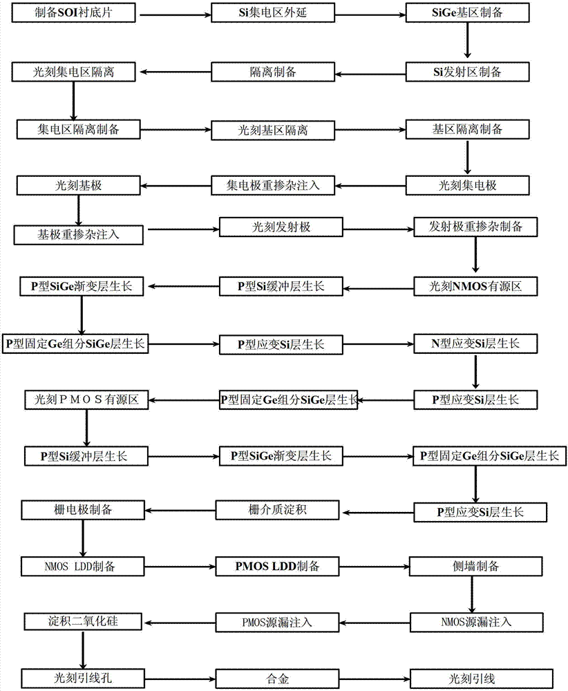
[0127] Embodiment 1: Preparation of a mixed crystal plane SOIBiCMOS integrated device and circuit based on a back-channel process with a channel length of 22 nm, the specific steps are as follows:

[0128] Step 1, SOI substrate material preparation.

[0129] (1a) Select N-type doping concentration as 1×10 15 cm -3 The Si wafer with a crystal plane of (110), the surface is oxidized, the thickness of the oxide layer is 0.5μm, as the underlying base material, and hydrogen is injected into the base material;

[0130] (1b) Choose the P-type doping concentration as 1×10 15 cm -3 The Si wafer with a crystal plane of (100), the surface of which is oxidized, and the thickness of the oxide layer is 0.5μm, as the base material of the upper layer;

[0131] (1c) Use chemical mechanical polishing (CMP) process to polish the surface of the lower layer and the upper layer of the base material after hydrogen injection;

[0132] (1d) SiO on the surface of the lower and upper base materials after polishin...

Embodiment 2

[0203] Embodiment 2: Preparation of a mixed-plane SOI BiCMOS integrated device and circuit based on a back-channel process with a channel length of 30 nm, the specific steps are as follows:

[0204] Step 1, SOI substrate material preparation.

[0205] (1a) Select the N-type doping concentration as 3×10 15 cm -3 Si wafer with a crystal plane of (110), the surface is oxidized, and the thickness of the oxide layer is 0.75μm, as the underlying base material, and hydrogen is injected into the base material;

[0206] (1b) Choose the P-type doping concentration as 3×10 15 cm -3 The Si wafer with a crystal plane of (100), the surface is oxidized, and the thickness of the oxide layer is 0.75μm, which is used as the base material of the upper layer;

[0207] (1c) Use chemical mechanical polishing (CMP) process to polish the surface of the base material of the lower layer and the upper layer after hydrogen injection;

[0208] (1d) SiO on the surface of the lower and upper base materials after poli...

Embodiment 3

[0279] Embodiment 3: Preparation of a mixed-surface SOI BiCMOS integrated device and circuit based on a back-channel process with a channel length of 45 nm, the specific steps are as follows:

[0280] Step 1, SOI substrate material preparation.

[0281] (1a) Choose N-type doping concentration as 5×10 15 cm -3 The Si wafer with a crystal plane of (110), the surface is oxidized, and the thickness of the oxide layer is 1μm, as the underlying base material, and hydrogen is injected into the base material;

[0282] (1b) Choose the P-type doping concentration as 5×10 15 cm -3 The Si wafer with a crystal plane of (100), the surface of which is oxidized, and the thickness of the oxide layer is 1μm, as the base material of the upper layer;

[0283] (1c) Use chemical mechanical polishing (CMP) process to polish the surface of the lower layer and the upper layer of the base material after hydrogen injection;

[0284] (1d) SiO on the surface of the lower and upper base materials after polishing 2 R...


PUM

PropertyMeasurementUnit
Thicknessaaaaaaaaaa
Thicknessaaaaaaaaaa
Thicknessaaaaaaaaaa

Abstract

The invention discloses a mixed crystal plane silicon-on-insulator (SOI) bipolar complementary metal oxide semiconductor (BiCMOS) integrated device based on a square channel process and a preparation method. The method comprises the following steps of: preparing an SOI substrate, continuously growing N-Si, P-SiGe and N-Si layers on the SOI substrate, preparing an deep groove isolator, forming a collector, a base and an emitter contact area, and forming a SiGe heterojunction bipolar transistor (HBT) device; photo-etching an active area of a p-channel metal oxide semiconductor (PMOS) device, continuously growing 7 layers of materials in the active area, preparing a drain and a grid, and forming the PMOS device; photo-etching a groove of an active area of an n-channel metal oxide semiconductor (NMOS) device, continuously growing 4 layers of materials in the active area, preparing a grid dielectric layer and grid polycrystalline, and forming the NMOS device; and photo-etching lead holes, alloying, photo-etching leads, and thus forming the mixed crystal plane SOI BiCMOS integrated device and a mixed crystal plane SOI BiCMOS integrated circuit of which CMOS conductive channels are 22 to 45 nanometers based on the square channel process. By fully using the characteristic of mobility anisotropy of a strain Si material, the mixed crystal plane SOI BiCMOS integrated circuit with enhanced performance is prepared at the temperature between 600 and 800 DEG C.

Description

Technical field [0001] The invention belongs to the technical field of semiconductor integrated circuits, and in particular relates to a mixed crystal plane SOI BiCMOS integrated device based on a back-shaped channel process and a preparation method. Background technique [0002] The integrated circuit that appeared in 1958 is one of the most influential inventions of the 20th century. Based on this invention, microelectronics has become the basis of existing modern technology, accelerating the change of the knowledge and information process of human society, and also changing the way of thinking of human beings. It not only provides humans with powerful tools to transform nature, but also opens up a broad space for development. [0003] In the contemporary era of highly developed information technology, microelectronics technology represented by integrated circuits is the key to information technology. As the fastest growing, most influential, and most widely used technology in ...

Claims


Application Information

Patent Timeline
IPC IPC(8): H01L27/06H01L21/8249
Inventor 胡辉勇宋建军张鹤鸣王斌吕懿宣荣喜舒斌郝跃
Owner XIDIAN UNIV
Why Eureka
Try Eureka