Single-sided electrode polycrystalline silicon thin film solar cell and manufacturing method thereof
A polysilicon thin film, solar cell technology, applied in the direction of circuits, electrical components, final product manufacturing, etc., can solve the problem of difficult to achieve the structure size, and achieve the effect of easy mass production, material saving, and thickness reduction.
- Summary
- Abstract
- Description
- Claims
- Application Information
AI Technical Summary
Problems solved by technology
Method used
Image

Examples
Embodiment 1
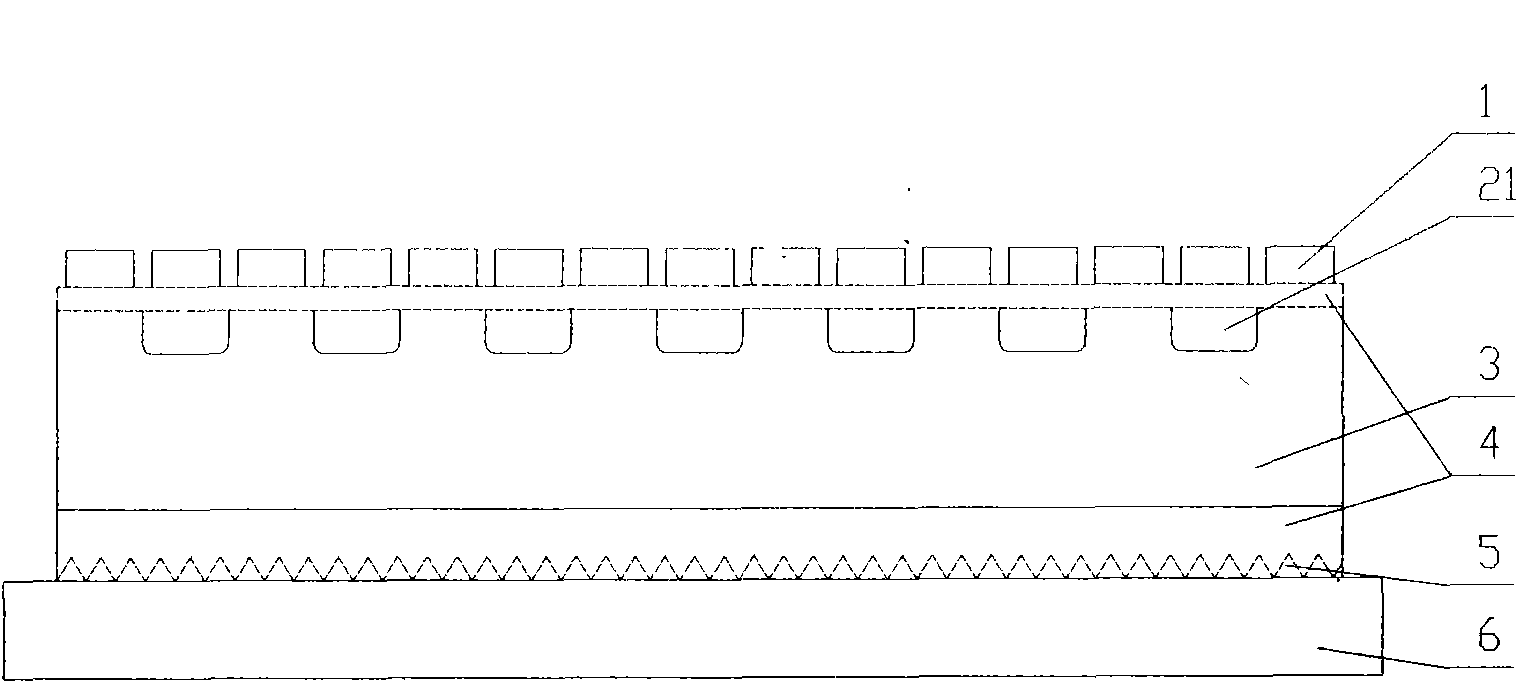
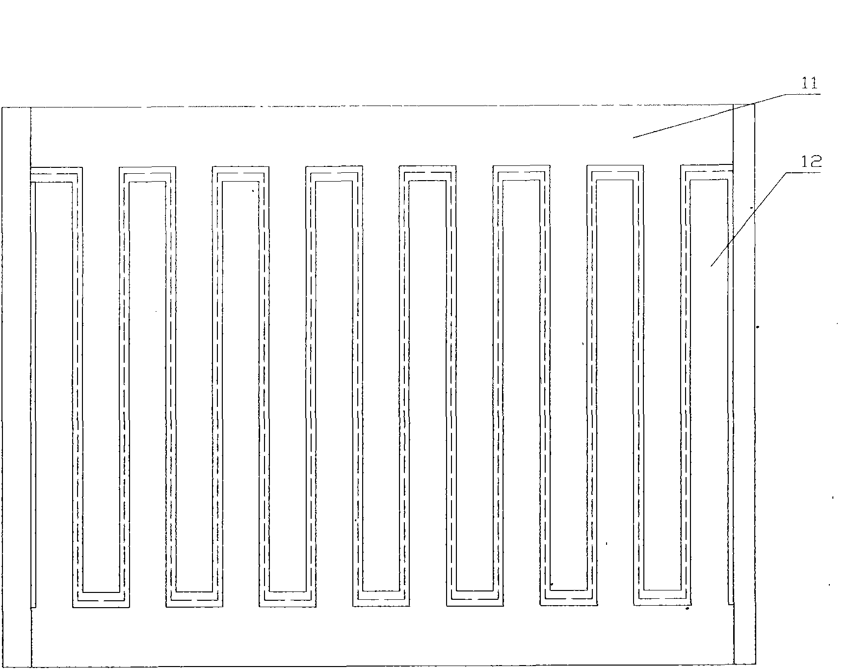
[0040] Embodiment one: as attached Figure 1 , Figure II As shown, a piece of ultra-clear glass of 300×300×3.0 mm is selected as the single-side electrode polysilicon thin-film solar cell substrate 6 . A layer of about 20nm SiO is placed on the surface of ultra-clear glass 2 Make the barrier and passivation composite film 4, and set the textured structure 5 at the interface where the film contacts with the ultra-clear glass. An N-type polysilicon film 3 with a thickness of 15 μm is provided on the composite film. Set P-type comb-like doping 2 inside the polysilicon film to form a PN junction 21 with a doping depth of 0.5 μm and a width of 0.5 mm, and set comb-like aluminum electrodes 11 and 12 at the comb-like doping position and the undoped position respectively , as the negative and positive electrodes of the solar cell, the width of the electrodes is determined according to the width of the PN junction to ensure that the positive and negative electrodes are not in contac...
Embodiment 2
[0042]Embodiment 2: A piece of ultra-clear glass with a size of 300×300×3.0 mm is selected as the single-side electrode polysilicon thin-film solar cell substrate. Make the surface of the glass into a suede structure, then set a layer of about 20nm SiNX on the surface of the ultra-clear glass as a barrier and passivation composite film, and set a layer of P-type polysilicon film with a thickness of 10 μm on the composite film. N-type grid-like doping 2 is set inside the crystalline silicon film to form a PN junction with a doping depth of 1 μm and a width of 0.5 mm. Grid-like silver-aluminum electrodes are respectively set at the grid-like doping position and the undoped position to serve as solar energy. For the positive and negative electrodes of the battery, the width of the electrodes is determined according to the width of the PN junction to ensure that the positive and negative electrodes are not in contact.
Embodiment 3
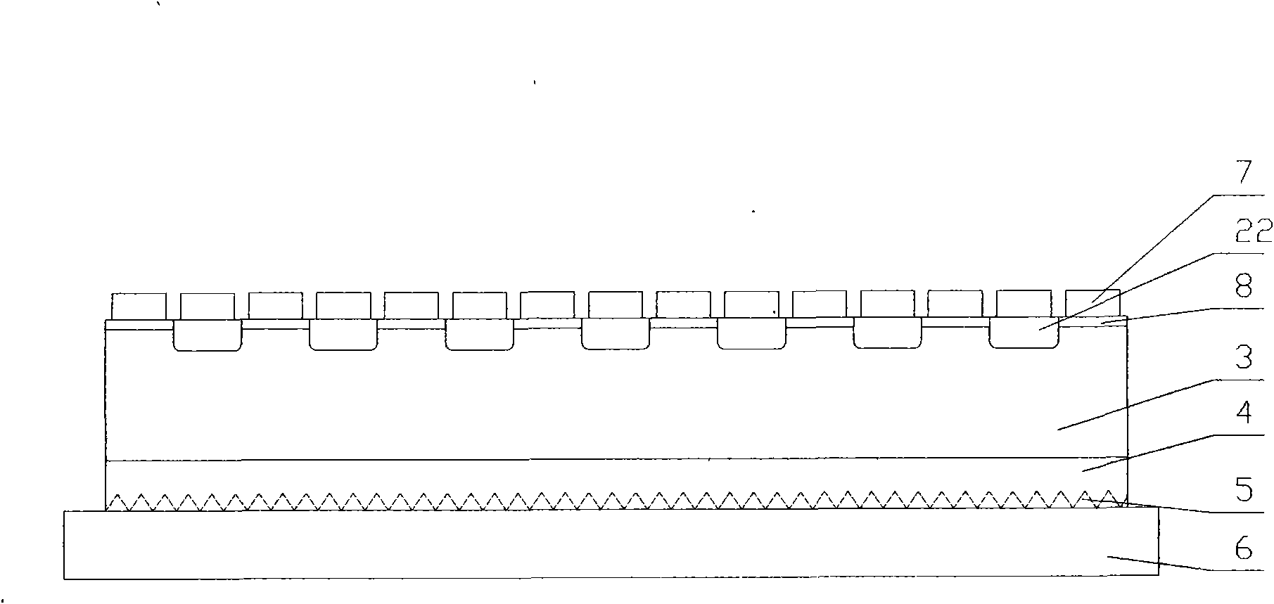
[0043] Embodiment three: as attached Figure three , attached Figure four As shown, a piece of ultra-clear glass with a size of 100×100×3.0 mm is selected as the single-side electrode polysilicon thin-film solar cell substrate 6 . Then set a layer of about 30nm SiN on the surface of the ultra-clear glass x +SiO2 2 A barrier and passivation composite film 4 is made, and a textured structure 5 is provided at the joint of the interface. A layer of N-type polycrystalline silicon film 3 with a thickness of 10 μm and a low doping concentration of 10 μm is provided above the composite film, and then a P-type grid-shaped doping is arranged on it to form a grid-shaped PN junction 22 with a doping depth of 1 μm and a width of 0.05 mm. . Grid-shaped silver electrodes 71 and 72 are respectively arranged at the grid-shaped doped position and the undoped position, as the negative conductive electrode and the positive conductive electrode of the solar cell, and a layer of thickness less...
PUM
| Property | Measurement | Unit |
|---|---|---|
| thickness | aaaaa | aaaaa |
| depth | aaaaa | aaaaa |
| thickness | aaaaa | aaaaa |
Abstract
Description
Claims
Application Information
 - R&D
- Intellectual Property
- Life Sciences
- Materials
- Tech Scout
- Unparalleled Data Quality
- Higher Quality Content
- 60% Fewer Hallucinations
Browse by: Latest US Patents, China's latest patents, Technical Efficacy Thesaurus, Application Domain, Technology Topic, Popular Technical Reports.
© 2025 PatSnap. All rights reserved.Legal|Privacy policy|Modern Slavery Act Transparency Statement|Sitemap|About US| Contact US: help@patsnap.com