Method and device for preparing solar cell surface gate electrodes by using light induction plating

A light-induced electroplating and solar cell technology, which is applied to circuits, electrical components, semiconductor devices, etc., can solve problems such as unsuitable solar cell technology and difficult light-induced electroplating, and achieve the effect of improving service life and overcoming warping deformation

Active Publication Date: 2015-05-20
YUNNAN UNIV
View PDF4 Cites 0 Cited by
  • Summary
  • Abstract
  • Description
  • Claims
  • Application Information

AI Technical Summary

Problems solved by technology

Ronald H. Micheels and others achieved a 10μm Cu gate coating on pure P-type silicon, but this method is not suitable for solar cell technology
There are two reasons: 1. The semiconductor solution junction electric field caused by the energy band structure of silicon makes it possible to achieve direct light-induced electroplating on P-type silicon at present, while the mainstream crystalline silicon solar cells in the market are mainly based on N-type 2. For a small number of solar cells (N-type solar cells) with a P-type surface as the light-receiving surface in the market, due to the existence of a PN junction, it will form a reverse power supply (that is, to the preset The electrode surface provides holes), and it is also difficult to achieve direct light-induced electroplating

Method used


Image

  • Method and device for preparing solar cell surface gate electrodes by using light induction plating
  • Method and device for preparing solar cell surface gate electrodes by using light induction plating
  • Method and device for preparing solar cell surface gate electrodes by using light induction plating

Examples


Embodiment 1

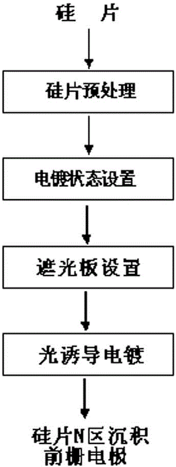
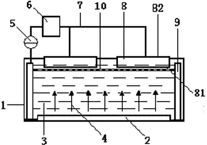
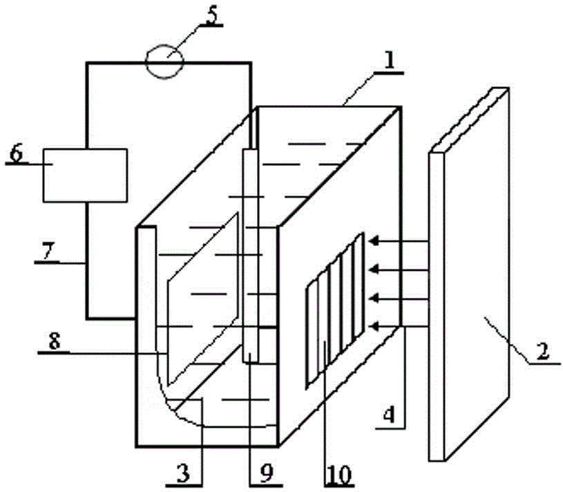
[0042] Inject the prepared 0.01mol / L Co metal ion light-induced electroplating solution into the electroplating pool, and electrically connect the battery silicon chip that has undergone texturing, diffusion, etching, dephosphorization, and back electrode preparation to the electroplating pool and its control circuit In the process, the back electrode of the silicon wafer of the battery is connected to the counter electrode of Co and the power circuit, the position of the silicon wafer of the battery is fixed and the surface of the N area is kept parallel to the surface of the electroplating liquid, and the surface of the N area of ​​the silicon wafer is immersed in the electroplating liquid. Set a grid-shaped shading plate between the surface of the N-zone of the battery silicon wafer and the fluorescent light source and ensure that the surface of the N-zone is parallel, start the light source, and let the light pass through the grid-shaped shading plate to irradiate the surfac...

Embodiment 2

[0044] With the Ni metal ion electroplating solution of 1mol / L as the light-induced electroplating solution, with the Ni electrode as the counter electrode, with natural light as the light source, according to the same process steps as in Example 1, prepare the grid-shaped electrode of the silicon wafer of the battery, and then use the light-induced Electroplating and ordinary electroplating methods, a layer of Cu metal is electroplated on the solar cell grid electrode to strengthen the grid electrode, and the effect is good. After testing, the grid-shaped electrode is firm, the resistivity is lower than that of the grid-shaped electrode prepared by the prior art, the aspect ratio is large, and the effective working area of ​​the battery is large. Compared with the comparison sample of the solar cell prepared by screen printing, the short-circuit current is increased by 5.23% , the open circuit voltage increased by 0.046%, and the fill factor increased by 0.24%.

Embodiment 3

[0046] With the Ni metal ion electroplating solution of 1mol / L as light-induced electroplating solution, with Ni electrode as counter electrode, with natural light as light source, according to the procedure step identical with embodiment 1, prepare battery silicon chip grid-shaped electrode, through detecting grid-shaped The electrode is strong, the resistivity is lower than the grid electrode prepared by the prior art, the aspect ratio is large, and the effective working area of ​​the battery is large. Compared with the comparison sample of the solar cell prepared by screen printing, the short-circuit current is increased by 2.30%, and the open-circuit voltage is increased. 0.046%, and the fill factor increased by 0.18%. This embodiment is in support of the previous embodiments without opting for enhanced plating.


PUM


Abstract

The invention discloses a method and a device for preparing grid electrodes on the surface of solar cells by light-induced electroplating. The method of the invention includes silicon chip pretreatment, electroplating state setting, light-shielding plate setting, light-induced electroplating process, and metal ions are directly deposited on the surface of the silicon chip by light-induced electroplating to form grid electrodes. The device of the present invention includes an electroplating pool, a light source, a wire, and a counter electrode. The bottom of the electroplating pool is provided with a light source, and the two sides of the electroplating pool are provided with counter electrodes. The counter electrode is connected to the back electrode of the silicon wafer. The bottom or lower side of the tank is provided with a drain and / or heating device, and the upper part of the electroplating tank is provided with a grid-shaped shading plate and placed under the surface of the N-region of the silicon wafer. The invention realizes the direct electroplating preparation of the grid-shaped electrode on the silicon wafer of the solar cell, without the need for slotting and pre-setting the seed layer process in the traditional method, reduces the production cost, and overcomes the small aspect ratio and contact resistance of the existing screen printing technology And the shortcomings of high bulk resistance and low efficiency.

Description

technical field [0001] The invention belongs to the technical field of electrochemistry, further belongs to the technical field of solar cell processing electrochemistry, and in particular relates to a method and a device for preparing solar cell surface grid electrodes by light-induced electroplating. Background technique [0002] Since the successful development of silicon PN junction solar cells by Chapin, Fuller and Pearson in 1954, devices using the p-n junction photovoltaic effect have been improved and evolved for more than half a century, and have developed into a class of solar cells with various geometric structures and corresponding manufacturing processes. However, crystalline silicon solar cells are still the mainstream of the photovoltaic industry today. [0003] The grid-shaped electrode of the crystalline silicon solar cell is responsible for collecting photo-generated electrons. Since it is on the light-receiving surface, it is made into a grid-like structur...

Claims


Application Information

Patent Timeline
Patent Type & Authority Patents(China)
IPC IPC(8): C25D7/12C25D5/02H01L31/0224
Inventor 刘铸肖辉徐哲冯苑飞
Owner YUNNAN UNIV
Why Eureka
Try Eureka