

Functional material with CuO and In2O3 micro-nano heterogeneous periodic structure and preparation method thereof
Patent Information
- Authority / Receiving Office
- CN · China
- Patent Type
- Applications(China)
- Current Assignee / Owner
- JILIN UNIV
- Publication Date
- 2012-10-24
- Estimated Expiration
- Not applicable · inactive patent
Smart Images
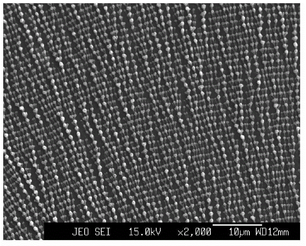
Figure 1 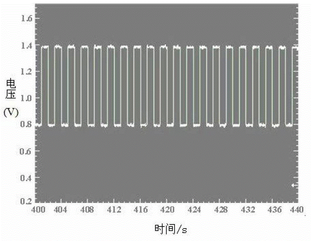
Figure 2 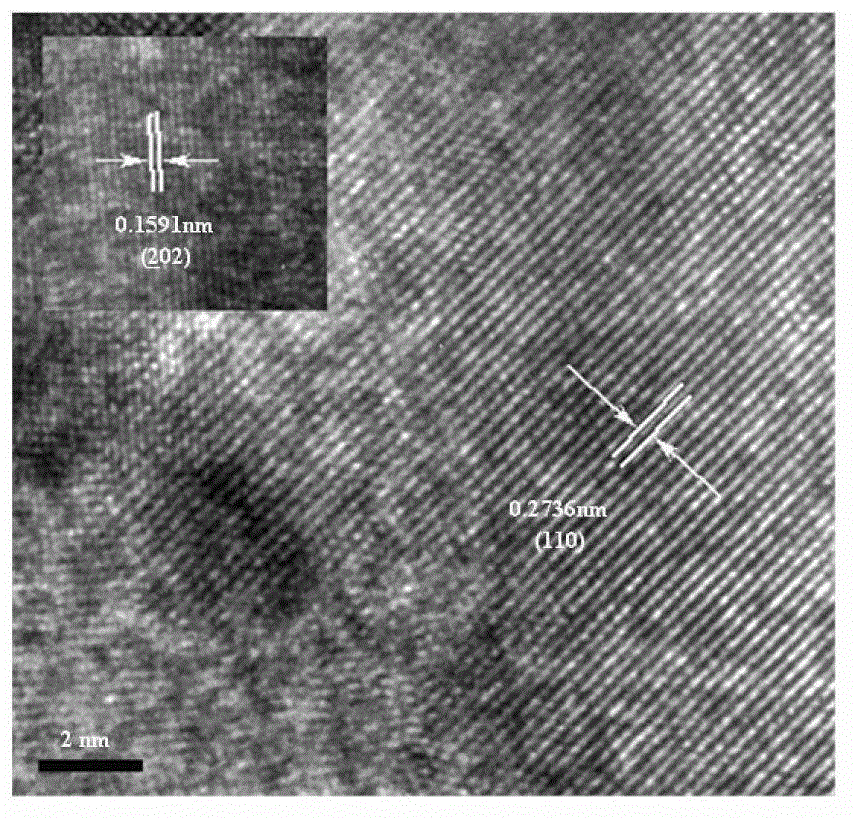
Figure 3
Abstract
Description
technical field
[0001] The invention belongs to the technical field related to semiconductor heterostructure functional materials, and relates to the method of electrochemical deposition to prepare In 2 o 3 And related technologies of CuO micro-nano heterogeneous periodic structure functional materials. Background technique
[0002] Functional nanomaterials have always been concerned by people, especially the preparation of semiconductor micro-nano heterostructure materials with good photoelectric and gas-sensing properties is the current research focus. A semiconductor heterostructure is a structure that combines two different types of semiconductor materials. The electronic behavior in this structure, including light irradiation, temperature, and the interaction between gas and electrons, and other physical properties are similar to those of a single semiconductor material. obviously different. In recent years, the research on many semiconductor oxide functional materia...